You are currently viewing SemiWiki as a guest which gives you limited access to the site. To view blog comments and experience other SemiWiki features you must be a registered member. Registration is fast, simple, and absolutely free so please,
join our community today!
WP_Term Object
(
    [term_id] => 157
    [name] => EDA
    [slug] => eda
    [term_group] => 0
    [term_taxonomy_id] => 157
    [taxonomy] => category
    [description] => Electronic Design Automation
    [parent] => 0
    [count] => 4531
    [filter] => raw
    [cat_ID] => 157
    [category_count] => 4531
    [category_description] => Electronic Design Automation
    [cat_name] => EDA
    [category_nicename] => eda
    [category_parent] => 0
    [is_post] =>
)
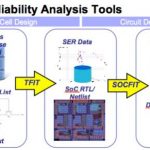
As we get down to smaller and smaller process nodes, the problem of soft errors becomes increasingly important. These soft errors are caused by neutrons from cosmic rays, alpha particles from materials used in manufacture and other sources. For chips that go into systems with high reliability this is not something that can be ignored.… Read More
One of the most useful ways to learn about an EDA tool is to talk with other users that have experience with that tool. IC Place and Route tools are complex and yet necessary to implement every SoC designed today, so at DAC in just two weeks you have a chance to hear first-hand from several P&R tool users. To get a better idea about these… Read More
Nvidia designs some of the most powerful graphics chips and systems in the world, so I’m always eager to learn more about their IC design methodology. This week I’ve had the chance to talk with Ting Ku, Director of Engineering at Nvidia about his DAC talkin the Apache booth in exactly two weeks from today. Registration… Read More
As I have mentioned before, Cliosoft is the biggest little company in EDA with the most talked about products on SemiWiki. At DAC, ClioSoft will introduce integrated SOS design management (DM) solutions providing revision control, design management and multi-site team collaboration for Aglient Technologies’ Advanced Design… Read More
My 8 years as an IC circuit designer were at the transistor-level, so if that interests you as well then consider what there is to see from Cadence at DAC this year. IC design technology is changing quickly, so keeping up to date is important for your job security and continual education goals.
Here’s what I would recommend attending… Read More
Last week I talked to Eileen You of Samsung-SSI to get a preview on what they will be talking about at Apache’s customer theater at DAC. Their presentation is titledThe Life of PI: SoC Power Integrity from Early Estimation to Design Sign-off. The ‘PI’ stands for Power Integrity.
Samsung-SSI’s operations… Read More
Today Cadence announced Tempus, their new timing signoff solution. This has been in development for at least a couple of years and has been built from the ground up to be massively parallelized. Not just that different corners can be run in parallel (which is basically straightforward) but that large designs can be partitioned … Read More
In a complex semiconductor market today, characterized by ever increasing design size and complexity, long design cycle, rapid technological advancement, intense competition, pricing pressure, small window of opportunity, development and cross-functional teams spread across the globe and multiple design partners including… Read More
Invarian is an interesting EDA company that sees a niche market opening in the physical verification space. There are a number of converging factors driving this opportunity. Electromigration and voltage-drop for full-chip analysis demands SPICE level accuracy with fast runtimes. Invarian solves that problem with macro … Read More
Funny story, @ #49DAC I saw Aart with a very relaxed look on his face looking at the exhibit hall and in my mind he was thinking, “Mine, all mine!” But I digress……. Synopsys is the #1 EDA company for a reason and here is the supporting data for that hypothesis:
Synopsys is committed to accelerating Innovation… Read More


Podcast EP357: How Gonka is Changing the Way AI is Accessed with David Liberman