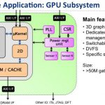
I love it when my Acura goes months and months without any major repair issue or computer-related glitches. Cars or networks only become reliable when they are designed and built for reliability. Freescale designs SoCs for advanced automotive and networking applications, and their engineers know much about the topics of power,… Read More
Electronic Design Automation
Chip and I/O Modeling for System-level Power Noise Analysis and Optimization
Cornelia Golovanovworks at LSI Corp in Pennsylvania and is an EMI expert that provides EDA tool and methodology advise to design groups. She earned a PhD in microelectronics and radioelectricity from the Institut national polytechnique de Grenoble, and joined Lucent out of school 12 years ago. We had a chance to talk by phone about… Read More
Jasper Low Power Verification App
Today, Jasper announced their new Jasper-Gold Low Power Verification App. This is focused on verifying low power designs with multiple power domains, voltage islands, power shutoff, clock shutoff, and all the other techniques used for reducing power. Of course power is the main driver of SoC design these days, whether it is for… Read More
SOCFIT, Circuit Level Soft Error Analysis
I blogged recently about reliability testing with high energy neutron beams. This is good for getting basic reliability data but it is not really a useful tool for worrying about reliability while the chip is still being designed and something can be done about it.
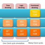
That is where IROC Technologies SOCFIT tool comes in. It takes all… Read More
UVM/SystemVerilog: Verification and Debugging
At DAC in just three weeks you can learn about which EDA vendors are supporting the latest UVM 1.1d (Universal Verification Methodology) standard as defined by Accellera. One of those EDA vendors is Aldec, and they have a 45 minute technical session that you can register for online. Space will fill up quickly, so get signed up sooner… Read More
A random walk down OS-VVM
Unlike one prevailing theory of financial markets, digital designs definitely don’t function or evolve randomly. But many engineers have bought into the theory that designs can be completely tested randomly. Certainly there is value to randomness, exercising all combinations of inputs, including unexpected ones a designer… Read More
Tektronix at #50DAC
If we grew up in similar eras you will know Tektronix as a company that manufactures test and measurement devices. Every lab I was in during high school and college had Tek oscilloscopes and logic analyzers. At #50DAC however, attendees that visit Tektronix will experience firsthand RTL simulation-level visibility to multi-FPGA… Read More
Cliosoft CEO on Design Collaboration Challenges!
Cliosoft was one of the first SemiWiki subscribers and it is a pleasure to work with them. They have one of the busiest landing pages with more than 30 articles authored by Daniel Payne, Paul McLellan, and myself. Srinath and I have lunch occasionally and exchange ideas, observations, and experiences:
Q: What are the specific design… Read More
A Big Boost for Equivalency Checking
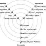
Thirty years ago in 1983 Professor Daniel Gajski and Kuhn created the now famous Y-Chart to show the various levels of abstraction in electronic system design:
We can still use this Y-Chart today because it still pertains to how engineers are doing their SoC designs. Along the Behavioral axis there is a need to know that each level… Read More
iDRM Brings Design Rules to Life!
Much awaited, automatic tool for DRM (Design Rule Manual) and DRC (Design Rule Check) deck creation is here now! I am particularly excited to know about this because I had been hearing for its need (in different context) from the designers with whom I was working to improve their design productivity through the use of our EDA tools… Read More


Silicon Insurance: Why eFPGA is Cheaper Than a Respin — and Why It Matters in the Intel 18A Era