You are currently viewing SemiWiki as a guest which gives you limited access to the site. To view blog comments and experience other SemiWiki features you must be a registered member. Registration is fast, simple, and absolutely free so please,
join our community today!
WP_Term Object
(
    [term_id] => 157
    [name] => EDA
    [slug] => eda
    [term_group] => 0
    [term_taxonomy_id] => 157
    [taxonomy] => category
    [description] => Electronic Design Automation
    [parent] => 0
    [count] => 4364
    [filter] => raw
    [cat_ID] => 157
    [category_count] => 4364
    [category_description] => Electronic Design Automation
    [cat_name] => EDA
    [category_nicename] => eda
    [category_parent] => 0
    [is_post] =>
)
One of the benefits of using high-level synthesis is obviously the ease of writing some algorithms in SystemC since it is at a higher level than RTL (that’s why we call it high-level synthesis!). But a second benefit is at the verification level. Since a lot of the verification gets done at the SystemC level, less needs to be done at … Read More
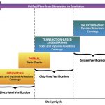
Speaking from experience, it is very difficult to get an OEM customer to talk about how they actually use standards and vendor products. A new white paper co-authored by Broadcom lends insight into how a variety of technologies combine in a flow from IP block simulation verification with assertions to complete SoC emulation with… Read More
Harish Aepalais part of the Design Closure Methodology group at LSIand he recently talked about his ASIC handoff experience in a webinar. Harish works with logic and physical synthesis, timing constraints, RTL analysis and formal verification.
One challenge with ASIC handoff has been getting through design closure with the… Read More
The company Nvidiais synonymous with designing all things video and GPU, so I watched Ting Ku, director of engineering at an archived webinar today talk about: Comprehensive Layout-based ESD Check Methodology with Fast Full-chip Static and Macro-level Dynamic Solutions.… Read More
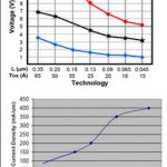
Switched-capacitor (SC) circuits are ubiquitous in CMOS mixed-signal ICs. Thermal noise, introduced by MOS switches and active amplifier circuitry, is the major performance limiter in these circuits. This webinar reviews analysis techniques to accurately analyze the noise performance of switched-capacitor circuits … Read More
The EDA tool space has been booming in this new “mobile era” of computing. As the world transitions to system-on-chip design methodologies, and as more teams are developing even more products for an ever-broadening set of end markets, the demand for ever more sophisticated design tools has only continued to skyrocket.… Read More
This is a live Silicon Valley event and yes there is such a thing as a free lunch. This is the first in a series of live SemiWiki collaborative events. I strongly believe that, especially in the age of social media, real world experience is key to the collaboration required to be successful in modern day semiconductor design. This is… Read More
In the spring of 1984, Mark Flomenhoft, Ph.D., approached Aki Fujimura, Randy Smith, and Steve Teig, to join him in developing a business plan to create a new EDA place and route (P&R) company. The three young software engineers all worked at Trilogy Systems Corporation where Mark was a director in the design automation department.… Read More
In the beginning of this decade there was a lot of buzz around 3D chip manufacturing. Many EDA tools were developed to facilitate semiconductor designs in 3D space. Naturally, we are moving to the edge on 2D without much room to further squeeze transistors and interconnect. However, lately I haven’t heard much about 3D products.… Read More
18 months ago I blogged about how the mobile revolution that we enjoy today is really enabled by EDA software and IP in the hands of SoC designers, yet very few EDA and Semi IP companies had mobile-ready web sites. In that past 18 months we’ve witnessed only a handful of companies migrate to mobile-friendly web sites, the most… Read More


Quantum Computing Technologies and Challenges