You are currently viewing SemiWiki as a guest which gives you limited access to the site. To view blog comments and experience other SemiWiki features you must be a registered member. Registration is fast, simple, and absolutely free so please,
join our community today!
WP_Term Object
(
    [term_id] => 157
    [name] => EDA
    [slug] => eda
    [term_group] => 0
    [term_taxonomy_id] => 157
    [taxonomy] => category
    [description] => Electronic Design Automation
    [parent] => 0
    [count] => 4439
    [filter] => raw
    [cat_ID] => 157
    [category_count] => 4439
    [category_description] => Electronic Design Automation
    [cat_name] => EDA
    [category_nicename] => eda
    [category_parent] => 0
    [is_post] =>
)
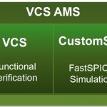
Digital verification engineers on SoC designs have adopted many techniques to help ensure first silicon success: using compiled simulators, constrained random test, simulation farms, SystemVerilog methodology, and self-checking testbenches. AMS verification has tended to be ad-hoc or sharply divided into separate analog… Read More
Light has become integral part of most of the electronic devices we use today in any sphere of influence; personal, entertainment, consumer, automotive, medical, security, and industrial and so on. It’s obvious; along with IoT (Internet-of-Things) devices, the devices to illuminate and display things will play a major role… Read More
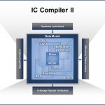
EDA start-up companies often have the advantage over established vendors by being able to start from scratch, instead of having to maintain some legacy code that no longer is competitive. But what happens when the established vendor decides to rewrite their IC implementation tools from scratch? In this case it’s good news,… Read More
The annual Design Automation Conference (DAC) is a big deal and should be of interest to students considering a career in developing software to help automate some of the toughest design and verification challenges in SoC design. Maybe the cost of attending and traveling to DAC is an issue for you. The organizers of DAC are continuing… Read More
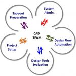
For most of my career, I worked as a CAD and design flow engineer. In the fall of 2012, I moved to a different role, as an applications and support manager at ClioSoft Inc. In my opinion, this was a very good opportunity for me to work with other CAD engineers and teams.
Having worked with different CAD teams in my career, I have often felt… Read More
As an example of the need for real-world reliability metrics, consider a modern automobile. We can already buy a car with parking assistance, collision avoidance, autonomous braking and adaptive cruise control features. These new features depend on video image processing that requires high-performance SoC components where… Read More
Mentor Graphics acquired Berkeley Design Automation this morning. The details of the deal were unannounced. This is a strong move by Mentor to challenge Cadence and Synopsys in the nanometer analog/mixed-signal market and nanometer memory characterization market, respectively. Mentor not only acquires the technology and… Read More
DAC is in the first week of June in San Francisco as I’m sure you already know if you are reading this. Historically DAC has focused on electronic design automation (EDA) and embedded software and systems (ESS). This year there are three new areas: automotive, Intellectual Property (IP) and security.
Automotive
Ever increasing… Read More
MEMS design and fabrication is highly complex in the sense that the fabrication process heavily depends on the design, unlike IC fabrication which has a standard set of processes. A slight change in MEMS design can alter its fabrication steps to a large extent. For example, setting device parameters such as capacitance or linear… Read More
There is clearly a lot of hype about the Internet of Things (IoT) right now, but also it is clear that it will be a real market. In fact, it already is with various medical, fitness and home-appliance products already available. At CES in January, wearables was probably the biggest trend. That doesn’t always pan out (3D TV was… Read More


Chemical Origins of Environmental Modifications to MOR Lithographic Chemistry