Usually these brief history pieces are totally written by the SemiWiki blogger whose name is at the top. Often me since that was how I prototyped book chapters (buy). Well, OK, I did actually write this but it is completely cribbed from a presentation earlier this week by Wally Rhines who gave a sort of keynote at the announcement of… Read More

Electronic Design Automation
Expert Constraint Management Leads to Productivity & Faster Convergence
The SoC designs of today are much more complex than ever in terms of number of clocks, IPs, levels of hierarchies, several modes of operations, different types of validations and checks for growing number of constraints at various stages in the design flow. As a semiconductor design evolves through several stages from RTL to layout,… Read More
U2U: Things You Might Not Know About TSMC
At Mentor’s U2U this afternoon I attended a presentation on TSMC’s use of Calibre PERC (it is a programmable electrical rule checker) for qualification of IP in TSMC’s IP9000 program. I’ve written about this before here. Basically IP providers at N20SOC, N16FF, and below are required to use PERC to guarantee… Read More
Mentor’s New Enterprise Verification Platform
I spent the morning at Mentor where they announced their new enterprise verification platform. This was a general announcement but was attended by a lot of the international press who were over on a GlobalPress tour (the event that used to take up camp at Chaminade).
But first Wally Rhines spent 30 minutes giving a nice overview of… Read More
Addressing MCU Mixed Signal Design Challenges
The emerging market for IoT and wearable devices are designed with mixed-signal IP that includes: embedded CPU, flash, analogue and radio.EDA and IP companies have recently worked together to allow us to design an MCU with mixed-signal IP blocks more efficiently. This morning I attended a webinar with presenters from ARMand … Read More
IP Reuse and Management in Monterey!
One of the benefits of being part of SemiWiki is building relationships with a wide variety of companies covering every semiconductor design application imaginable. We are blessed, absolutely. Another benefit of being part of SemiWiki are the invitations to attend, participate, and even organize events such as EDPS. Last year… Read More
A New, Free, Web-Based EDA Toolset in the Cloud
In the 1990’s there was a push to build EDA frameworks, however they all failed because no user wanted to be locked into one EDA vendor tool flow. Fast forward to 2014 and there’s an emerging trend to use web-based EDA tools as a framework, instead of downloading and installing software to your desktop or device. I just… Read More
A New Digital Place and Route System
IC place and route tools can be very high-priced EDA software to purchase or lease, so there’s some good news for AMS designers that need an affordable digital place and route tool for their mostly analog designs. Today the team at Tanner EDAannounced a totally new place and route system has been added to their Schematic Driven… Read More
SEMulator3D 2014 – New Enhancements for Virtual Fabrication in the 3D IC Era

A Virtual Platform for any kind of design or manufacturing in any discipline of science or engineering (electrical, mechanical, aeronautics etc.) must be able to provide an accurate representation of an actual design/product in a fraction of time and cost it takes to build working prototypes. In the case of semiconductors at … Read More
Semiconductor IP Validation Gets Faster
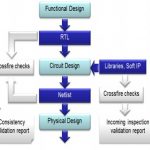
Semiconductor IP continues to grow in use for SoC design, and many chips can now use hundreds of IP blocks from multiple vendors. Validating the quality of the IP blocks is an important step in the design process, and you could perform manual validation and inspection of each new IP block at the expense of time and engineering effort.… Read More
Musk’s Orbital Compute Vision: TERAFAB and the End of the Terrestrial Data Center