You are currently viewing SemiWiki as a guest which gives you limited access to the site. To view blog comments and experience other SemiWiki features you must be a registered member. Registration is fast, simple, and absolutely free so please,
join our community today!
WP_Term Object
(
    [term_id] => 157
    [name] => EDA
    [slug] => eda
    [term_group] => 0
    [term_taxonomy_id] => 157
    [taxonomy] => category
    [description] => Electronic Design Automation
    [parent] => 0
    [count] => 4181
    [filter] => raw
    [cat_ID] => 157
    [category_count] => 4181
    [category_description] => Electronic Design Automation
    [cat_name] => EDA
    [category_nicename] => eda
    [category_parent] => 0
    [is_post] =>
)
One of the highlights of the TSMC 2013 Open Innovation Platform® Forum was the Partner Award Ceremony. TSMC awarded Berkeley Design Automation (BDA) with the TSMC Open Innovation Platform’s Partner of the Year Award 2013 for joint development of 16nm FinFET design infrastructure. I talked with Ravi Subramanian, BDA CEO,… Read More
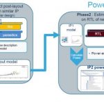
At DAC this year there was a presentation from Samsung titled, “Profile-based Architecture Power Modeling Methodology for AP/SoC Product”. I’ve been using Samsung Smart Phones for the past four generations, so was very curious about how they have managed to improve the average battery life from less than… Read More
When new restaurants open they sometimes have what is called a ‘soft opening’ where they open a few days earlier than the official opening night. They are less busy since nobody knows they are open yet, maybe the whole menu isn’t available and expectations may be lower. Of course, Broadway productions also often… Read More
It was an interesting webinar I attended, presented by STMicroelectronicson how they are benefited in power saving and thermal dissipation by using FDSOI technology and also by using PowerArtist in their design. So, it’s an advantage from both sides – semiconductor technology and semiconductor design tool. It’s worth attending… Read More
70% of today’s ASIC and SoC designs are being prototyped on FPGAs. Everybody knows that. But, did you know that automating the process of converting what could be thousands of ASIC “golden” files into FPGA-friendly versions can mean big savings in a large design?… Read More
Engineers are always looking to improve the efficiency of how they work, but don’t want to sacrifice accuracy in the process. This is true in the world of semiconductor process development, where traditional build-and-test cycles are both time and resource intensive. But what if there was a way to do certain steps in a ‘virtual’… Read More
In one of my favorite movies, Brad Pitt utters the only question that matters in baseball or technology management in the face of uncertainty: “Okay, good. What’s the problem?” Not surprisingly in that scene, as the question circles the table of experts used to doing things the old way, not a single one can answer it correctly in the… Read More
One of TSMC’s two big Silicon Valley events each year is the Open Innovation Platform (OIP) Forum. This year it is on Tuesday October 1st. It is in the San Jose Convention Center and starts at 9am (registration opens at 8am). Pre-registration to attend is now open here or click on the image to the right.
From 9.10 to 9.40 is the … Read More
What Mentor Said at ITCby Beth Martin on 09-26-2013 at 4:47 pmCategories: EDA
At the ITC test conference in early September, Mentor made three announcements. ITC is a big event for Mentor’s test group, and where they usually roll out their new tools and capabilities. The indefatigable Steve Pateras was captured on film describing them.
I’ve summarize Mentor’s three announcements and added… Read More
Ashok Mehtahas designed processors at DEC and Intel, managed ASIC vendor relationships, verified networks SoCs, directed engineers at AMCC, and used SystemVerilog since it’s inception. He recently authored a book: SystemVerilog Assertions and Functional Coverage. The book is available in both hardcover and Kindle… Read More


Moore’s Law Wiki