Apple has redefined three industries within a decade: media player with the iPod, mobile handset with the iPhone and portable computers with the iPad. If there is anything common in these three game-changing product development stories other than Apple, it’s the ARM footprint. Even now the technology media is abuzz with speculation… Read More

Electronic Design Automation
Open Source Software Platform Fuels Automotive Innovation
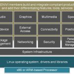
These days, most of the innovative concepts in our cars are driven by electronics; not only infotainment systems, but also instrument clusters, safety systems including ADAS (Advanced Driver Assistance Systems), information displays, night vision, airbags, backup camera, stability control, and so on. The upcoming connected… Read More
Vertical NAND Flash
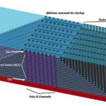
You may know that up until now NAND flash has been a planar technology. But just as with SoC processes where we have had to go vertical to FinFETs, NAND flash has reached the limitations of scaling in the 20nm nodes and is also going vertical. It is not just a lithography issue but there are also reliability and voltage scaling issues.… Read More
Apple’s Ax Chronicle
In April 2008, Apple baffled the semiconductor industry by acquiring the system-on-chip (SoC) pioneer PA Semi for US$278 million. The acquisition, took place at the height of the iPhone fever, left the technology and trade media with an endless suite of guessing games. In the end, it was just about Apple’s quest for having… Read More
Intel and the Intel-of-Things
When I joined Calma in 1982, Intel was a small company making microprocessor chips in a crowded marketplace. They had scored big with IBM who was using their 8088 in the very first personal computer. Wind River was a hatchling with David Wilner and Jerry Fiddler working out of a rented warehouse in Berkeley – I know, I hung out… Read More
Wow: Synopsys v. Mentor Update!
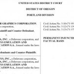
As a reminder, the Synopsys v. Mentor drama started when Synopsys filed a Complaint for Declaratory and Injunctive Relief on the same day (September 27, 2012) as they entered into an agreement to acquire emulation provider EVE (ZeBu emulator systems), which competes with Mentor’s Veloce family of emulators. Apparently, upon… Read More
SoCs in New Context Look beyond PPA
If we look back in the last century, performance and area were two main criteria for semiconductor chip design. All design tools and flows were concentrated towards optimizing those two aspects. As a result, density of chips started increasing and power became a critical factor. Now, Power, Performance and Area (PPA) are looked… Read More
Silvaco Swallows Invarian
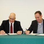
Yesterday, Silvaco announced that it has acquired Invarian Inc. Details of the transaction were not disclosed.
Who is Invarian? They are a recognized leader in block-level to full-chip sign-off analysis for complex, high-performance ICs. Their unique methodology utilizes a parallel architecture and concurrent power-voltage-thermal… Read More
Full Spectrum Analog FastSPICE Useful for RF Designs on Bulk CMOS
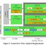
It has been about a year since the acquisition of Berkeley Design Automation by Mentor Graphics. Berkeley was doing quite well in the somewhat crowded SPICE simulator market. In many respects they broke new ground for high speed and accurate SPICE simulators. Since the acquisition we know that former Berkeley executives are now… Read More
ARM & Cadence IP Partnership for Faster SoC Design

IP vendors always try to create differentiation, especially when designing protocol based IP. You can differentiate by building the most performing controller but you will probably miss the expectation of these customers who don’t search for performance but just compliance to a specific standard. Or the vendor may want to design… Read More
Silicon Insurance: Why eFPGA is Cheaper Than a Respin — and Why It Matters in the Intel 18A Era