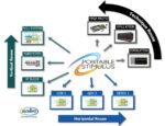
Tom Fitzpatrick, a Strategic Verification Architect at Mentor, a Siemens Business, has worked on IEEE and Accellera standards like Verilog 1364, System Verilog 1800, UVM 1800.2 and is Vice Chair of the Portable Stimulus working group, so when I heard that he was doing a webinar on how PSS can be used to create better stimulus for … Read More
Electronic Design Automation
WEBINAR: Transitioning from Live to Virtual Events
The foundation of SemiWiki.com has always been to transition live semiconductor related events to an easy to digest digital format via a worldwide online semiconductor community. SemiWiki is staffed by working semiconductor professionals that transform live events, press releases, whitepapers, webinars and other collateral… Read More
High Speed SerDes Design and Simulation Webinar Replay from Mentor
Over the years SerDes (serializer/deserializer) based connections have proliferated into just about every connection within and among computing systems. Years ago, parallel interfaces were the most common method of moving data, but issues of signal integrity, synchronization and power simply became too much for the required… Read More
The Problem with Reset Domain Crossings
Design complexities in reset, like everything else in big SoC designs, has become incredibly complex, for all sorts of reasons. Long, long ago reset was something you just did once, when you turned the power on. Turn on, then hold reset for some amount of time until everything is in a known starting state, and off you go. Nice and simple.… Read More
SEMI Takes the Jim Hogan and Simon Butler Conversation Virtual
As I originally reported a few weeks ago, the Jim Hogan fireside chat with Methodic’s CEO and founder Simon Butler was moved to a virtual event on May 1. The event was produced by the Electronic System Design (ESD) Alliance, a SEMI Strategic Technology Community. Bob Smith, executive director of ESDA, moderated the event. I am happy… Read More
Cadence – Redefining EDA Through Computational Software
Based on what I’m seeing, I believe Cadence is looking at the world a bit differently these days. I first reported about their approach to machine learning for EDA in March, and then there was their white paper about Intelligent System Design in April. It’s now May, and Cadence is shaking things up again with a new white paper entitled… Read More
How to Modify, Release and Update IP in 30 Minutes or Less
I had the opportunity to attend a ClioSoft webinar recently on the topic of IP traceability. ClioSoft provides a broad range of tools for design data management and IP reuse. Entitled The New Trend in IP Traceability that IP Developers and Design Managers Rely On, the webinar was presented by Karim Khalfan, director of applications… Read More
DFT Innovations Come from Customer Partnerships
There is an adage that says that quality is not something that can be slapped on at the end of the design or manufacturing process. Ensuring quality requires careful thought throughout development and production. Arguably this adage is more applicable to the topic of Design for Test (DFT) than almost any other area of IC development… Read More
Linux for Medical Devices Q&A
As I have mentioned before SemiWiki gets to meet some very smart people and here is another one. Scot Morrison has an MS degree in Aerospace Engineering from MIT specializing in control systems. Today he is the general manager of the Embedded Platform Solutions Division at Mentor, a Siemens business. Scot oversees the Linux®, Nucleus®,… Read More
Slash Tapeout Times with Calibre in the Cloud
I’ve spent many years in the ASIC business, and I’ve seen my share of complex chip tapeouts. All of these projects share one important challenge – compute requirements explode when you get close to the finish line. Certain tools need to run on the full-chip layout for final verification and the run times for those tools can get excessively… Read More


Silicon Insurance: Why eFPGA is Cheaper Than a Respin — and Why It Matters in the Intel 18A Era