You are currently viewing SemiWiki as a guest which gives you limited access to the site. To view blog comments and experience other SemiWiki features you must be a registered member. Registration is fast, simple, and absolutely free so please,
join our community today!
WP_Term Object
(
    [term_id] => 19172
    [name] => Chiplet
    [slug] => chiplet
    [term_group] => 0
    [term_taxonomy_id] => 19172
    [taxonomy] => category
    [description] =>
    [parent] => 0
    [count] => 230
    [filter] => raw
    [cat_ID] => 19172
    [category_count] => 230
    [category_description] =>
    [cat_name] => Chiplet
    [category_nicename] => chiplet
    [category_parent] => 0
    [is_post] =>
)
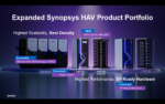
Last week, Synopsys announced an expansion of their Hardware-Assisted Verification (HAV) portfolio to accelerate semiconductor design innovations. These advancements are designed to meet the increasing demands of semiconductor complexity, enabling faster and more efficient verification across software and hardware… Read More
The dominance of GPUs in AI workloads has long been driven by their ability to handle massive parallelism, but this advantage comes at the cost of high-power consumption and architectural rigidity. A new approach, leveraging a chiplet-based RISC-V vector processor, offers an alternative that balances performance, efficiency,… Read More
Dave Hwang joined Alchip in 2021 as General Manager of Alchip’s North America Business Unit. He also serves as Senior Vice President, Business Development. Prior to join Alchip, Dave served as Vice President, Worldwide Sales and Marketing for Global Unichip and in a variety of management and technical roles at TSMC. He holds… Read More
Anna Fontanelli, CEO of MZ Technologies, is a silicon executive with more than 35 years of expertise in managing complex R&D organizations/programs to give birth to innovative EDA technologies. Strong communication skills and proven ability to lead distributed, cross functional teams in international environments.… Read More
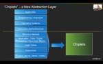
The semiconductor industry is facing a paradigm shift. Traditional scaling, once driven by Moore’s Law, is slowing down. For years, moving to smaller process nodes led to lower transistor costs and better performance. However, scaling from node to node now offers fewer benefits as wafer costs rise much more than the historical… Read More
Keysight, with deep roots tracing back to Hewlett-Packard, has long been at the forefront of innovation in electronic design and testing. It manufactures electronics test and measurement equipment and software. The company also owns its own foundry and makes custom chips and packages for its instrumentation business. Many… Read More
Predictions in technology adoption often hinge on a delicate balance between technical feasibility and market dynamics. While business considerations play a pivotal role, the technical category reasons for the success or failure of a prediction are more tangible and often easier to identify—if scrutinized with care. However,… Read More
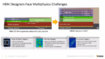
3D design with high-bandwidth memory stacks (HBM) has become essential for leading edge semiconductor systems in multiple applications. Hyperscalers depend on large AI accelerator cores supported by 100GB or more of in-package HBM to handle trillion parameter AI models. Autonomous Drive (AD) vehicles may handle smaller … Read More
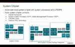
The automotive industry is evolving rapidly with the increasing demand for intelligent, connected, and autonomous vehicles. Central to this transformation are System-on-Chip (SoC) designs, which integrate multiple processing units into a single chip for managing everything from safety systems to in-car entertainment.… Read More
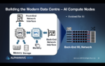
Artificial intelligence (AI) has revolutionized data center infrastructure, requiring a reimagining of computational, memory, and connectivity technologies. Meeting the increasing demand for high performance and efficiency in AI workloads has led to the emergence of innovative solutions, including chiplets, advanced… Read More


Enhancing Multi-Domain System Simulation with FMI Co-Simulation