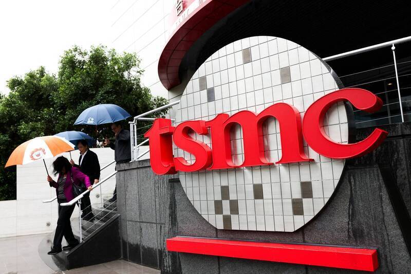
 TSMC manufactures wafers in the United States, but currently still needs to ship them back to Taiwan for packaging and testing. Future plans include a dual-track model of building its own facilities and strategic partnerships. (Bloomberg photo)
According to sources in the semiconductor supply chain, TSMC's US wafer fab is accelerating its progress. The advanced packaging plant cannot wait to rebuild outside the current plant area. In order to integrate with the front-end wafer fab and shorten the time to serve customers, TSMC plans to convert the land of the planned sixth phase fab (P6 fab) into an advanced packaging (AP) plant. If the construction goes smoothly, it is expected to be installed as early as the end of 2027 and enter the pre-production stage.
TSMC mass-produces wafers in the US, but currently still needs to ship them back to Taiwan for packaging and testing. Future plans involve a dual-track approach: self-built facilities and strategic partnerships. Previously, TSMC partnered with US packaging and testing company Amkor, with Amkor investing in and building a factory in Taiwan to provide back-end packaging and testing services. Amkor has already started construction on a factory near TSMC, with production expected to begin in 2028. Considering the urgent need for a faster timeline, recent reports suggest that the self-built facility plan may be repurposed for an advanced packaging plant on the P6 plant site.
TSMC announced this year that it will increase its investment in Arizona, USA, by a total of approximately US$165 billion, including the original US$65 billion investment and an additional US$100 billion, to build six wafer fabs, two advanced packaging plants and one research and development center.
TSMC's first-phase US plant began mass production in the fourth quarter of 2024, using a 4-nanometer process to manufacture products for customers such as Apple, AMD, and Nvidia. The second-phase plant has been completed and is currently under construction, with production expected to begin using a 3-nanometer process in the third quarter of 2027. The third-phase plant has been started ahead of schedule and will switch to 2-nanometer and A16 processes, striving to start trial production in 2028 and mass production in 2029.
TSMC plans to establish a gigafab in Arizona and is therefore looking for a second large site to support future expansion needs. It is projected that by 2030, the proportion of advanced process capacity manufactured in the United States with a process size of less than 2 nanometers will reach 30%.

台積電美國P6廠用地 傳將轉建先進封裝廠 - 自由財經
〔記者洪友芳/新竹報導〕半導體供應鏈傳出,台積電美國晶圓廠加速進展,後段先進封裝廠等不及在目前廠區以外重新建廠,為了就近結合前段晶圓廠,縮短服務客戶時效,台積電預計將在規劃第六期廠(P6廠)用地
 ec.ltn.com.tw
