I enjoy learning and writing about new technologies closely connected to our personal and working lives (the kind you could explain to your Mom or a neighbor). So naturally I’m interested in AI, communication and security as applied to the home automation, transportation, virtual, augmented and mixed reality, industry and so on – the burgeoning electronification of our world.
But there’s been a glaring gap in my coverage. All of this clever technology would have little or no value if it couldn’t sense key environmental factors – our orientation, acceleration, temperature, pressure, sound – the list is endless. This is a rich universe of innovation that, so far, I have only looked at peripherally. Now I’m getting more interested in this domain, and I’m starting with how Mentor/Tanner supports the design of the key elements at the heart of these sensors – microelectromechanical systems or MEMS – and the circuits that connect those systems to the rest of the electronics.

Take microphones. Not karaoke mics, but the ones you’ll find in smartphones, Amazon Echo speakers and the latest generation earbuds and hearing aids, supporting “Siri” and similar commands. Many of these are made by Knowles (about who I’ve written recently). The mic is a MEMS design, fabricated on silicon, but it doesn’t look much like conventional silicon circuits.
One basic structure might be a couple of membranes separated by a layer of air; as sound waves hit one of the membranes it flexes, changing the capacitance between the membranes. A different structure depends on sound waves flexing piezo-electric mechanical structures, generating electrical signals. Either way, analog circuitry next to the device detects the response. Then all that’s left is a little signal conditioning, converting the analog signal to digital for better noise immunity and you have yourself a microphone.
OK, gross oversimplification but that’s the general principal and it highlights one key aspect of MEMS: they are (at minimum) micromechanical devices with gaps between layers, cantilevered beams or host of other possibilities, all designed to respond to targeted ambient influences in a way that can be converted into electrical signals and passed on for analysis. Another big difference from conventional semiconductor lithography is that shapes of elements in these devices can be pretty much anything (Knowles microphones use circular membranes for example), where more conventional lithography at these dimensions is rectlinear.
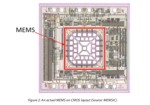
As you might imagine, while manufacturing techniques for MEMS may start with the same techniques used for conventional semiconductors, these must be augmented with specialized micro-machining processes. Designing these systems is also challenging. If you thought analog + digital was hard, here you have to design and verify mechanical + analog + digital systems. Tanner is well-known for its expertise in this domain and certainly seems to be widely used. They cite Knowles and MEMSIC as customers; I’m sure there are more they haven’t chosen to share.
The tool-suite supports an interesting parallel flow – for MEMS, for analog and for digital circuitry (these may or may not be on the same die). I won’t bore you with the analog and digital flows except to mention that Mentor/Tanner have tools to support each step of design/analysis and implementation. For MEMS system design and simulation Tanner provides MEMS PRO. System simulation uses the Tanner circuit sim tools together with a behavioral model of the MEMS, derivable directly from your design when you start design from their library of composable models. And of course you can run full mixed-level simulation for all three domains.
For implementation, again Mentor Tanner provide tools for analog and digital flows. They don’t mention compatibility with 3rd-party flows though I’d guess they make some allowance for this, since the MEMS layout is unlikely to intermix with circuit layout. The MEMS implementation is of course Tanner-based, including evolving the design to 3D-solid modeling based on the target foundry and process. This model can then be taken into detailed finite-element analysis for mechanical, thermal, electromagnetic and fluidics analysis. And for layout verification, the Tanner tools include DRC checking which checks for the special features unique to MEMS layouts. (I’m assuming you’ll still use Calibre for the rest of the circuitry.)
The economics behind delivering sensors as packaged parts is also interesting. Expected unit prices for individual sensors are very low (<$1) so sensor-makers are motivated to combine multiple sensor functions. Combining a 3-axis gyroscope, 3-axis accelerometer and 3-axis compass in one device gives you a 9-axis sensor, especially important in VR and similar functions.
Taking this further, smart sensors are becoming routine in ADAS, combining one or more sensing functions with a controller to locally process and reduce data along with a communication interface. This may be more to reduce traffic on auto ethernets than to improve vendor ASPs, but the outcome is the same. Sensor fusion is a hot topic and that means more sensors and more functionality around those sensors must be integrated into a package.
Of course the Tanner tools are not only valuable for sensors. You can also build actuators, pumps, whatever you might need. Maybe that will be another blog. Meantime you can learn more about how Tanner/Mentor enable building these sensors from these two white papers: Sensors are Fundamental to New Intelligent Systems and Autonomous Drive Requires Smart Sensor Systems.
Share this post via:


Comments
2 Replies to “Mentor-Tanner Illuminate MEMS Sensing, Fusion”
You must register or log in to view/post comments.