You are currently viewing SemiWiki as a guest which gives you limited access to the site. To view blog comments and experience other SemiWiki features you must be a registered member. Registration is fast, simple, and absolutely free so please,
join our community today!
Amidst frequently changing requirements, time pressure and demand for high accuracy, it is imperative that EDA and design companies look at time consuming processes in the overall design flow and find alternatives without losing accuracy. High Frequency Analysis of IC designs is one such process which is traditionally based… Read More
These days when we talk of SoC verification, what comes to our mind immediately is VirtualPlatform. Of course with the increasing size, complexity and different styles of designs, it is very much a need.
However, that is supported by actual verification engines and methodologies which are varying considerable with digital, … Read More
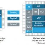
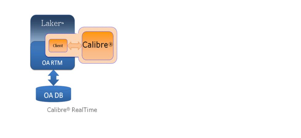
Mixed-Signal design is one of the very initial design methodologies, pioneered by Cadence with its lead in custom design; now taking centre space in the world of SoCs. Its growth is surmountable as it finds its place in most of the high growth electronics like smart phones, automotive applications, networks and communications,… Read More
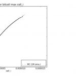
In 1990s when designs were small, I was seeing design and EDA community struggling to improve upon huge time taken to verify the circuits, specifically with Spice and the like. I was myself working on developing tool for transistor level static timing analysis (STA) mainly to gain on time (eliminating the need of exhaustive set … Read More
It has been a year since my article Semiconductor Landscape in Jan 2012 I wanted to look back into the major events over the year and then anticipate what’s in store going forward. What has happened over the year is much more than what I could foresee. Major consolidation in EDA space – Synopsys acquired Magma, SpringSoft, Ciranova,… Read More
We are all aware that at 28nm and below several types of complex layout effects manifest themselves into the design and pose a herculean task, with several re-spins to correct them at pre-tapeout. It’s apparent that the layout needs to be correct by construction at the very beginning during the design stage.
Having worked at Cadence… Read More
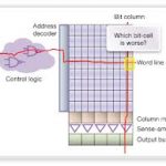
In today’s era, high performance mobile devices are asserting their place in every gizmos we play with and guess what enables them work efficiently behind the scene – it’s large chunks of memory with low power and high speed, packed as dense as possible. Ever growing requirement of power, performance and area led us to process nodes… Read More
Recently I was researching the keynote speeches of isQED (International Society for Quality Electronic Design) Symposium 2012 and saw the very first, great presentation, “Taming the Challenges in Advanced Node Design” by Tom Beckley, Sr. VP at Cadence. I know Tom very well as I have worked with him and I admire his knowledge, authority… Read More
In my last article I talked about the physical design aspect of 3D-IC. Now looking at its verification aspect, it spans through a wide spectrum of test at hardware as well as software level. The verification challenge goes much beyond that of a SoC which is at a single plane. Even a typical SoC that comprises of a processor core, memory… Read More
As I have been watching the developments in EDA and Semiconductor industry, it is apparent that we remain fragmented unless pushed to adopt a common standard mostly due to business reasons. Foundries are dictating on the rules to be followed by designs, thereby EDA tools incorporating them. Also, design companies needed to work… Read More


TSMC CoWoS versus Intel EMIB Semiconductor Packaging