
For advanced lithography used to shrink semiconductor device features according to Moore’s Law, resolution limits are an obvious consideration. It is often perceived that the resolution limit is simply derived from a well-defined equation, but nothing can be further from the truth.

Author: Fred Chen
The Complexities of the Resolution Limits of Advanced Lithography
How Line Cuts Became Necessarily Separate Steps in Lithography
Pretty much all the semiconductor nodes in the last two decades have had at least one layer where the minimum pitch pushes the limitation of the state-of-the-art lithography tool, with a k1 factor < 0.5, i.e., the half-pitch is less than 0.5*wavelength/numerical aperture. A number of published reports [1-4] have touched upon… Read More
CD-Pitch Combinations Disfavored by EUV Stochastics
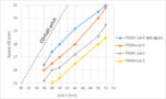
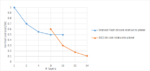
Ongoing investigations of EUV stochastics [1-3] have allowed us to map combinations of critical dimension (CD) and pitch which are expected to pose a severe risk of stochastic defects impacting the use of EUV lithography. Figure 1 shows a typical set of contours of fixed PNOK (i.e., the probability of a feature being Not OK due… Read More
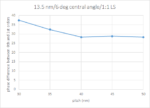
Impact of Defocus and Illumination on Imaging of Pitch
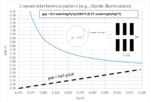
In an earlier article [1], the resolution limit for the space between paired features was described by the Rayleigh criterion of ~0.6 wavelength/numerical aperture, where the numerical aperture (NA) represented the sine of the largest angle for a ray focused from the lens to a point. It is also given by the radius of the lens divided… Read More
Toshiba Cost Model for 3D NAND
Toshiba (now known as Kioxia) was the first company to propose a 3D stacked version of NAND Flash memory called BICS [1]. BICS (BIt Cost Scalable) Flash used explicit process cost reduction based on depositing and etching multiple layers at once, avoiding multiple lithography steps. This strategy replaced the usual approach… Read More
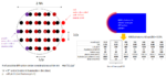
Smartphone Processor Trends and Process Differences down through 7nm
This comparison of smartphone processors from different companies and fab processes was originally going to be a post, but with the growing information content, I had to put it into an article. Here, due to information availability, Apple, Huawei, and Samsung Exynos processors will get the most coverage, but a few Qualcomm Snapdragon
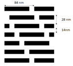
Fully Self-Aligned 6-Track and 7-Track Cell Process Integration

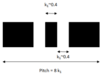
For the 10nm – 5nm nodes, the leading-edge foundries are designing cells which utilize 6 or 7 metal tracks, entailing a wide metal line for every 4 or 5 minimum width lines, respectively (Figure 1).
Figure 1. Left: a 7-track cell. Right: a 6-track cell.
This is a fundamental vulnerability for lithography, as defocus can change… Read More
Application-Specific Lithography: 20nm Flash, 3D XPoint, 3D NAND Bit Lines

Nonvolatile memory capacity reached 64 Gb levels when NAND Flash half-pitch reached 20 nm [1]. Having reached 14 nm [2], NAND Flash half-pitch is no longer being reduced, now that it has entered the 3D era. However, recently, 3D XPoint has found applications within the Optane platform [3]. The lithography for patterning 20 nm half-pitch… Read More
EUV faces Scylla and Charybdis
It is now time for the EUV community to realize they are caught between the proverbial Scylla and Charybdis. In Greek mythology, the two monsters terrorized ships that were unlucky enough to pass between them. By avoiding one, you approached the other.
S for Scylla, or Stochastics
Scylla was a former beautiful nymph turned into
Application-Specific Lithography: a 28 nm Pitch DRAM Active Area
In the recent DRAM jargon, “1X”, “1Y”, “1Z”, etc. have been used to express all the sub-20 nm process generations. It is almost possible now to match them to real numbers which are roughly the half-pitch of the DRAM active area, such as 1X=18, 1Y ~ 17, etc. At this rate, 14 nm is somewhere around


The Semiconductor Growth Numbers are Insane but the Real World Doesn’t Tally!