
There is growing awareness that EUV lithography is actually an imaging technique that heavily depends on the distribution of secondary electrons in the resist layer [1-5]. The stochastic aspects should be traced not only to the discrete number of photons absorbed but also the electrons that are subsequently released. The electron… Read More

Author: Fred Chen
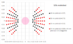
Spot Pairs for Measurement of Secondary Electron Blur in EUV and E-beam Resists
EUV’s Pupil Fill and Resist Limitations at 3nm
The 3nm node is projected to feature around a 22 nm metal pitch [1,2]. This poses some new challenges for the use of EUV lithography. Some challenges are different for the 0.33NA vs. 0.55NA systems.
0.33 NA
For 0.33 NA systems, 22 nm pitch can only be supported by illumination filling 4% of the pupil, well below the 20% lower limit for
Obscuration-Induced Pitch Incompatibilities in High-NA EUV Lithography
The next generation of EUV lithography systems are based on a numerical aperture (NA) of 0.55, a 67% increase from the current value of 0.33. It targets being able to print 16 nm pitch [1]. The High-NA systems are already expected to face complications from four issues: (1) reduced depth-of-focus requires thinner resists, which… Read More
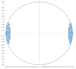
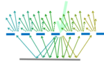
The Electron Spread Function in EUV Lithography
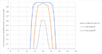
To the general public, EUV lithography’s resolution can be traced back to its short wavelengths (13.2-13.8 nm), but the true printed resolution has always been affected by the stochastic behavior of the electrons released by EUV absorption [1-5].
A 0.33 NA EUV system is expected to have a diffraction-limited point spread… Read More
Double Diffraction in EUV Masks: Seeing Through The Illusion of Symmetry
At this year’s SPIE Advanced Lithography conference, changes to EUV masks were particularly highlighted, as a better understanding of their behavior is becoming clear. It’s now confirmed that a seemingly symmetric EUV mask absorber pattern does not produce a symmetric image at the wafer, as a conventional DUV … Read More
Demonstration of Dose-Driven Photoelectron Spread in EUV Resists
As a consequence of having a ~13.5 nm wavelength, EUV photons transfer ~90% of their energy to ionized photoelectrons. Thus, EUV lithography is fundamentally mostly EUV photoelectron lithography. The actual resolution becomes dependent on photoelectron trajectories.
Photoelectron trajectories in EUV lithography were… Read More
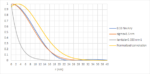
Adding Random Secondary Electron Generation to Photon Shot Noise: Compounding EUV Stochastic Edge Roughness
The list of possible stochastic patterning issues for EUV lithography keeps growing longer: CD variation, edge roughness, placement error, defects [1]. The origins of stochastic behavior are now well-known. For a given EUV photon flux into the resist, a limited fraction are absorbed. Since the absorption is less than 5% affected… Read More
EUV Resist Absorption Impact on Stochastic Defects
Stochastic defects continue to draw attention in the area of EUV lithography. It is now widely recognized that stochastic issues not only come from photon shot noise due to low (absorbed) EUV photon density, but also the resist material and process factors [1-4].
It stands to reason that resist absorption of EUV light, which is … Read More
Etch Pitch Doubling Requirement for Cut-Friendly Track Metal Layouts: Escaping Lithography Wavelength Dependence

The 5nm foundry node saw the arrival of 6-track standard cells with four narrow routing tracks between wide power/ground rails (Figure 1a), with minimum pitches of around 30 nm [1]. The routing tracks require cuts [2] with widths comparable to the minimum half-pitch, to enable the via connections to the next metal layer with the… Read More
Horizontal, Vertical, and Slanted Line Shadowing Across Slit in Low-NA and High-NA EUV Lithography Systems
EUV lithography systems continue to be the source of much hope for continuing the pace of increasing device density on wafers per Moore’s Law. Recently, although EUV systems were originally supposed to help the industry avoid much multipatterning, it has not turned out to be the case [1,2]. The main surprise has been the


RISC-V and AI: The Architecture Shift Is Now