You are currently viewing SemiWiki as a guest which gives you limited access to the site. To view blog comments and experience other SemiWiki features you must be a registered member. Registration is fast, simple, and absolutely free so please,
join our community today!
Britto Vincent of ProPlus Design Solutions met with me at DAC on Monday morning to talk about Design For Yield (DFY) and Analog Fast SPICE.
In 2011 ProPlus announced DFY tools where the technology came from IBM, it provides fast Monte Carlo results up to 3 sigma, then added NanoSpice for faster simulation results. Similar in approach… Read More
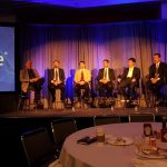
Wednesday morning I attended a panel discussion with: ARM, IBM, Cadence, GLOBALFOUNDRIES and Samsung.
The panelists all sang the same song of collaboration between EDA, IP and Foundry to enable 28nm, 20nm and even 14nm.… Read More
ARM and Synopsys are well-known physical IP companies however at DAC today I met with a lesser-known company named DXCORR that has some unique offerings for cache, multi-port memory and standard cell kicker libraries. I met with:… Read More
I arrived to a sunny San Francisco this afternoon, checked into my hotel then visited Moscone Center to pick up my Independent Media credentials. On the walk over I passed by Yerba Buena Gardens.… Read More
One year ago the annual share holder meeting at Mentor Graphics had tight security, a no-camera policy, and the drama of Carl Icahn the corporate raider successfully adding three new board members. Fast forward to today where two of Icahn’s board members were not even nominated, and Mentor added two new board members. I chatted… Read More
I first met Stuart at Mentor Graphics back in 1995 or so, and he is one of the most knowledgable persons around for all things Verilog.
Stuart Sutherland is the editor for the IEEE 1800 SystemVerilog standard, so if you’re attending DAC and care about SystemVerilog then consider attending the Birds of a Feather meeting held… Read More
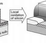
Have you ever heard of a Super Pillar Transistor? It’s one of many emerging 3D transistor types, like Intel’s popular FinFET device.
In the race to continuously improve MOS transistors, these new 3D transistor structures pose challenges to the established IC extraction tool flows.
Foundries have to provide an Effective… Read More
Last year when I visited Tanner EDA at DAC I heard about how they integrated the Analog FastSPICE circuit simulator from Berkeley DA.
This made sense to me because BDA has a good reputation for speeding up SPICE without compromising on accuracy, and Tanner users may want to mix and match tools from multiple EDA vendors.
This year they’ve… Read More
In April I blogged about a webinar on co-simulation hosted by Aldec and Tanner EDA where they showed how the RTL simulator (Riviera PRO) and SPICE simulator (T-Spice) had been connected together for IC designers wanting to do real AMS simulations.
The availability date of the co-simulation wasn’t clear, so today the press… Read More
Yesterday I met with Michael Buehler-Garcia, Director of Marketing at Mentor Graphics for Calibre in Wilsonville, Oregon to get an update on what’s coming up at DAC, the premier conference and trade show for our industry.
… Read More


Intel 18A vs Intel 18A-P: What Is the Difference and Why Does It Matter?