You are currently viewing SemiWiki as a guest which gives you limited access to the site. To view blog comments and experience other SemiWiki features you must be a registered member. Registration is fast, simple, and absolutely free so please,
join our community today!
Digital designers have been automating the functional verification process for many years now, however when you talk to an analog designer about how they do verification you quickly realize that the typical process is quite ad-hoc and little automated. Necessity does create an opportunity so the software engineers at Methodics… Read More
Social Media at Atrentaby Daniel Payne on 03-27-2014 at 11:01 pmCategories: EDA
Atrentais well-known for their SpyGlass software that enables SoC engineers to run early design analysis on RTL code and create a hardware virtual prototype for analysis prior to implementation. Visiting their website you quickly see that social media plays an important role in connecting with engineers as links for Facebook,… Read More
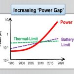
Power analysis and reduction for SoC designs is a popular topic because of our consumer electronics dominated economy, and the need to operate devices on a battery source for the maximum time before a recharge. Just from my desk I can see multiple battery-powered devices: Laptop, tablet, smart phone, e-book reader, bluetooth … Read More
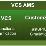
Digital verification engineers on SoC designs have adopted many techniques to help ensure first silicon success: using compiled simulators, constrained random test, simulation farms, SystemVerilog methodology, and self-checking testbenches. AMS verification has tended to be ad-hoc or sharply divided into separate analog… Read More
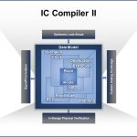
EDA start-up companies often have the advantage over established vendors by being able to start from scratch, instead of having to maintain some legacy code that no longer is competitive. But what happens when the established vendor decides to rewrite their IC implementation tools from scratch? In this case it’s good news,… Read More
The annual Design Automation Conference (DAC) is a big deal and should be of interest to students considering a career in developing software to help automate some of the toughest design and verification challenges in SoC design. Maybe the cost of attending and traveling to DAC is an issue for you. The organizers of DAC are continuing… Read More
The most successful EDA companies typically choose a domain where they have deep knowledge, then serve a few leading-edge customers that are willing to work with a start-up in exchange for early access to that new technology. The theory is that if you can satisfy the leading-edge customer then you can also satisfy the rest of the … Read More
Started in 2002 Carbon Design Systems has ESL (Electronic System Level) modeling and validation tools for complex SoC design. With their software you can:
- Perform system level model generation of existing and 3rd party IP directly from RTL for use in any virtual platform
- Do performance analysis & optimization of SoC architectures
…
Read More
3D TV has been all the rage over the past few years because of the added realism it offers the viewer, but there’s really not that much content that you can stream or play on a Blu-ray device. Wouldn’t it be cool if there was a box that could create 3D on the fly from a 2D stream or Blu-ray? This week I discovered that such a box… Read More
I first started using WordPress in 2008 after having written my own Content Management System (CMS) to build and manage web sites. WordPress is the number one CMS in the world, is just 10 years old, and is used by over 70 million users. What got me thinking about WordPress and EDA software companies was a recent book by Scott Burken, … Read More


Intel, Musk, and the Tweet That Launched a 1000 Ships on a Becalmed Sea