You are currently viewing SemiWiki as a guest which gives you limited access to the site. To view blog comments and experience other SemiWiki features you must be a registered member. Registration is fast, simple, and absolutely free so please,
join our community today!
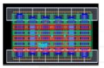
At SemiWiki we’ve written four times now about how TSMC is standardizing on a 3DIC physical flow with their approach called 3Dblox, so I watched a presentation from John Ferguson of Siemens EDA to see how their tool flow supports this with the Calibre tools. With a chiplet-based packaging flow there are new physical verification… Read More
On big chip design projects the logic verification effort can be larger than the design effort, taking up to 70% of the project time based on data from the 2022 Wilson Research Group findings. Sadly, the first silicon success rate has gone downwards from 31 percent to just 24 percent in the past 8 years, causing another spin to correct… Read More
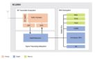
Nearly every week I read in the popular press another story of a major company being hacked: Twitter, Slack, LastPass, GitHub, Uber, Medibank, Microsoft, American Airlines. What is less reported, yet still important are hardware-oriented hacking attempts at the board-level to target a specific chip, using voltage Side-Channel… Read More
It’s January so time for me to review what I’ve found at CES this year that relates to cycling. Unlike last year when there were many last-minute cancellations from exhibitors, in 2023 it’s in-person and bigger than ever. The electrification of bikes continues, and many of these electronic devices are cloud… Read More
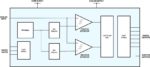
Sensors are inherently analog in nature, and they get digitized for processing by using an Analog to Digital Converter (ADC) block. At the recent IP SoC event I had the chance to see the presentation by Ken Potts, COO of Alphacore on their semiconductor IP for ADCs. I learned that Alphacore started out in 2012, now offering both standard… Read More
I first heard about High Level Synthesis (HLS) while working in EDA at Viewlogic back in the 1990s, and have kept watch on the trends over the past decades. Earlier this year Siemens EDA hosted a two day event, having speakers from well-known companies share their experiences about using HLS and High Level Verification (HLV) in their… Read More
Automotive engineers are familiar with the ISO 26262 standard, as it defines a process for developing functional safety in electronic systems, where human safety is preserved as all of the electronic components are operating correctly and reliably. Automotive electronics have now grown to cover dozens of applications, and… Read More
The world of analog cell design and migration is quite different from digital, because the inputs and outputs to an analog cell often have a continuously variable voltage level over time, instead of just switching between 1 and 0. Kenny Hsieh of TSMC presented on the topic of analog cell migration at the recent North American OIP … Read More
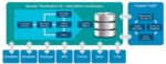
On November 10th I watched the presentation by L.C. Lu, TSMC Fellow & VP, as he talked about enabling system innovation with dozens of slides in just 26 minutes. TSMC is the number one semiconductor foundry in the world, and their Open Innovation Platform (OIP) events are popular and well attended as the process technology and… Read More
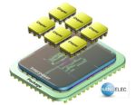
Before chiplets arrived, it seemed like designing an electronic system was a bit simpler, as a system on chip (SoC) methodology was well understood, and each SoC was mounted inside a package, then the packages for each component were interconnected on a printed circuit board (PCB). The emerging trend to design a 3D IC using chiplets… Read More


Captain America: Can Elon Musk Save America’s Chip Manufacturing Industry?