You are currently viewing SemiWiki as a guest which gives you limited access to the site. To view blog comments and experience other SemiWiki features you must be a registered member. Registration is fast, simple, and absolutely free so please,
join our community today!
One of the best things about being part of SemiWiki is the exposure to new technologies and the people behind them. SemiWiki now works with more than 35 companies and I get to spend time with each and every one of them. Much like I do, IROC Technologies works closely with the foundries and the top semiconductor companies so it was a pleasure… Read More
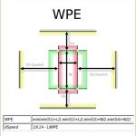
In advanced process technologies, electrical and timing problems due to variability can become a big issue. Due to various processing effects, a circuit performance (both speed and power) is dependent on specific layout attributes and can vary a lot from instance to instance. The accumulated effects can be severe to the point… Read More
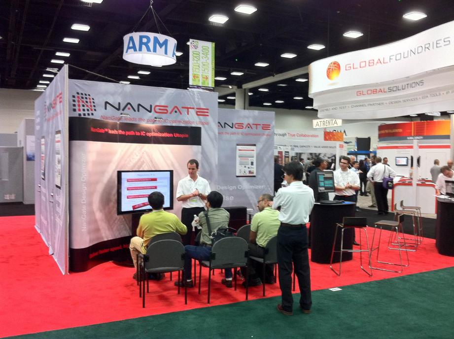
NanGate got started in 2004 by a group of engineers from Vitesse Semi and Intel. The technology and market idea was to address and solve the inherent shortcomings of standard cell based design as compared to full custom. Anyone having tried to push the performance of a standard cell design knows the frustration… if only I had a better… Read More
As I have mentioned before, Cliosoft is the biggest little company in EDA with the most talked about products on SemiWiki. At DAC, ClioSoft will introduce integrated SOS design management (DM) solutions providing revision control, design management and multi-site team collaboration for Aglient Technologies’ Advanced Design… Read More
Invarian is an interesting EDA company that sees a niche market opening in the physical verification space. There are a number of converging factors driving this opportunity. Electromigration and voltage-drop for full-chip analysis demands SPICE level accuracy with fast runtimes. Invarian solves that problem with macro … Read More
Funny story, @ #49DAC I saw Aart with a very relaxed look on his face looking at the exhibit hall and in my mind he was thinking, “Mine, all mine!” But I digress……. Synopsys is the #1 EDA company for a reason and here is the supporting data for that hypothesis:
Synopsys is committed to accelerating Innovation… Read More
Last week Berkeley Design Automation introduced a new Analog Characterization Environment (ACE) – a high-productivity system to ensure analog circuits meet all specifications under all expected operational, environmental, and process conditions prior to tapeout.
While standard cell characterization and memory characterization… Read More
One of the places you will be able to find me at the Design Automation Conference (DAC) is on the speaker panel for a Monday Tutorial – Winning in Monte Carlo: Managing Simulations Under Variability and Reliability. Having worked closely with TSMC, GLOBALFOUNDRIES, Solido Design Automation, and some of the top fabless semiconductor… Read More
Most EDA companies sell tools into the main chip design and implementation flow such as simulation, synthesis, place & route, custom design and mask data prep. Atrenta is different. Nothing the company sells is in this main design flow. Instead, Atrenta focuses on pre-synthesis design analysis and optimization. Everything… Read More
Cadence is a DAC anchor, everyone will visit their booth, so lets look at their technical sessions and put our agendas together. Lets start with the breakfast/lunch sessions because Cadence usually puts out quite a spread, we all gotta eat and free food tastes even better:
Has “Timing Signoff Innovation” Become an Oxymoron? What… Read More


Chemical Origins of Environmental Modifications to MOR Lithographic Chemistry