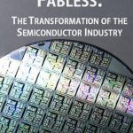
The generosity of the fabless semiconductor ecosystem never ceases to amaze me. Paul McLellan and I wrote a book for the greater good and now key members of our industry will make sure that 1,500 people at this year’s Design Automation Conference will get copies. As a special thank you to all of our supporters SemiWiki will be hosting… Read More
Author: Daniel Nenni
A Novel Approach to IC Design in the Cloud
Migration to cloud computing for scientific and engineering applications is inevitable. More specifically for IC design, the benefits are significant:
- Common IC design infrastructure to unburden each user from setting up and maintaining a separate infrastructure
- Cloud based IC design enables global collaboration among
More Moore or No More?
Moore’s is still the law, and device scaling remains the key focus of front-end process research, however next-generation technologies–and the Big Data, cloud computing world that supports mobile, IoT, and other next-gen applications–are the new drivers, bringing new demands and challenges running … Read More
Motley Fools Intel Investors Again!
It really is quite a racket. Investor bloggers spread semiconductor disinformation for $.01 per click, that coincidentally covers their stock positions, and I get paid $300 per hour to explain it to Wall Street. While I appreciate the opportunity to bond with the financial people, I do wonder how these bloggers sleep at night.… Read More
Variation-Aware Custom IC Design Best Practices
I’ve worked with Solido for 5 years, and it’s been a pleasure to watch the world’s top semiconductor companies and foundries adopt Solido software for their SPICE simulation flows.
Sub-28nm design starts are accelerating, growing from 150 in 2012 to 900 this year. The move to sub-28nm design nodes is being driven by consumer electronic… Read More
Can Intel be a Leading Semiconductor Foundry?
This is the third part of a series answering the most frequently asked questions I get from Wall Street. Please read the previous two articles on Intel’s Manufacturing Lead and Intel’s SoC Challenge before flaming me in the comment section. First let’s look at why there is a foundry business and go from there.
The big… Read More
Automotive Focus @ #51DAC!
For the first time in DAC history there is an automotive track. Being a car person myself this is exciting news. I had a quick chat with Anne Cirkel, Vice Chair of DAC, and she sent me the following information to get us prepared for our week in San Francisco. The weather is going to be great so plan accordingly!
Ever increasing feature… Read More
Atrenta @ #51DAC Must See!
Last year at DAC, we launched the RTL Signoff platform and our customers responded enthusiastically. We even had a few other EDA companies follow our lead. So what have we been up to since then?
Visit us at DAC this June and learn how we have expanded our industry leading RTL Signoff solutions to handle the next set of challenges in SoC… Read More
Intel’s SoC Challenge!
Innovation is the cornerstone of the semiconductor industry and as history has shown, the majority of semiconductor innovation has come from fabless companies. Apple computer is my favorite example since they went from selling mother boards to computer hobbyists in the 1970’s to being one of the largest and most influential … Read More
Intel’s Manufacturing Lead Explained
The calls from Wall Street keep coming with basically the same set of questions: “Does Intel really have a 2-3 year process lead? Can Intel lead the foundry segment? Can Intel Lead the Mobile SoC Segment?” The feeling amongst the buy and sell side investment people is that unless Intel can lead a market they will not stay in it… Read More


Siemens U2U 3D IC Design and Verification Panel