You are currently viewing SemiWiki as a guest which gives you limited access to the site. To view blog comments and experience other SemiWiki features you must be a registered member. Registration is fast, simple, and absolutely free so please,
join our community today!
Always in motion is the future. ~Yoda
For nearly ten years now, full-chip simulation engines have successfully used process models to perform OPC in production. New full-chip models were regularly introduced as patterning processes evolved to span immersion exposure, bilayer resists, phase shift masking, pixelated illumination… Read More
Managing Test Power for ICsby Beth Martin on 11-07-2011 at 12:17 pmCategories: EDA, Siemens EDA
The goal for automatic test pattern generation (ATPG) is to achieve maximum coverage with the fewest test patterns. This conflicts with the goals of managing power because during test, the IC is often operated beyond its normal functional modes to get the highest quality test results. When switching activity exceeds a device’s… Read More
Will Rogers said that an economist’s guess is liable to be as good as anyone’s, but with advanced-node optical lithography, I might have to disagree. Unlike the fickle economy, the distorting effects of the mask and lithographic system are ruled by physics, and so can be modeled.
In this installment, I’ll talk about two critical… Read More
Testing, testing… 3D ICsby Beth Martin on 10-06-2011 at 7:01 pmCategories: EDA, Siemens EDA
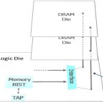
3D ICs complicate silicon testing, but solutions exist now to many of the key challenges. – by Stephen Pateras
The next phase of semiconductor designs will see the adoption of 3D IC packages, vertical stacks of multiple bare die connected directly though the silicon. Through-silicon vias (TSV) result in shorter and thinner… Read More
Wyatt Earp probably wasn’t thinking of OPC when he said, “Fast is fine, but accuracy is everything,” but I’ll adopt that motto for this discussion of full-chip OPC and post-OPC verification models.
Accuracy is the difference between the calibrated model prediction and the calibration wafer result. Accuracy depends on several… Read More
Can Your Router Handle 28 nm?by Beth Martin on 06-20-2011 at 7:11 pmCategories: EDA, Siemens EDA
With the adoption of the 32/28 nm process node, some significant new challenges in digital routing arise—including complex design rule checking (DRC) and design for manufacturing (DFM) rules, increasing rule counts, very large (1 billion transistor) designs. To meet quality, time-to-market, and cost targets, design teams… Read More
Dawn at the OASIS, Dusk for GDSIIby Beth Martin on 03-28-2011 at 1:53 pmCategories: EDA, Siemens EDA
For an industry committed to constant innovation, changes in any part of the design flow are only slowly adopted, and only when absolutely necessary. Almost 10 years ago, it became clear that shrinking process technologies would bring a massive growth of layout and mask data—rougly 50% per node. This avalanche of data seriously… Read More
In part I of this series, we looked at the history of lithography process models, starting in 1976. Some technologies born in that era, like the Concorde and the space shuttle, came to the end of their roads. Others did indeed grow and develop, such as the technologies for mobile computing and home entertainment. And lithography … Read More
With EUVL, Expect No Holidayby Beth Martin on 03-02-2011 at 1:12 pmCategories: EDA, Siemens EDA
For a brief time in the 1990s, when 4X magnification steppers suddenly made mask features 4X larger, there was a period in the industry referred to as the “mask vendor’s holiday.” The party ended before it got started with the arrival of sub-wavelength lithography, and we all trudged back to the OPC/RET mines. Since then, the demands… Read More
Evolution of process models, part Iby Beth Martin on 02-23-2011 at 1:15 pmCategories: EDA, Siemens EDA
Thirty five years ago, in 1976, the Concorde cut transatlantic flying time to 3.5 hrs, Apple was formed, NASA unveiled the first space shuttle, the VHS vs Betamax wars started, and Barry Manilow’s I Write the Songs saturated the airwaves. Each of those advances, except perhaps Barry Manilow, was the result of the first modern-era,… Read More








Silicon Insurance: Why eFPGA is Cheaper Than a Respin — and Why It Matters in the Intel 18A Era