For a brief time in the 1990s, when 4X magnification steppers suddenly made mask features 4X larger, there was a period in the industry referred to as the “mask vendor’s holiday.” The party ended before it got started with the arrival of sub-wavelength lithography, and we all trudged back to the OPC/RET mines. Since then, the demands for pattern correction have grown ever more onerous. But at long last, there may be an extreme ultraviolet light at the end of the lithography tunnel.
Extreme ultraviolet lithography (EUVL) is a strong candidate for 15nm node and below. While the 13.5nm EUV wavelength seems to imply a bit of an OPC vendor’s holiday, it’s shaping up to be quite the opposite situation. EUVL is introducing two major pattern-distorting effects at a magnitude never before seen: flare and mask shadowing. These effects combined create pattern distortions of several nanometers, and they vary in magnitude across the reticle in a complex yet predictable way. So, unpack your bags, there’s no holiday with EUVL.
EUV Lithography Patterning Distortions
There are several technical challenges for EUVL, but I’ll focus on just one: correcting pattern distortions unique to EUVL, specifically flare and mask shadowing.
Flareis an incoherent light produced by scattering from imperfections in the optical system, and it can degrade image contrast and worsen control of CD. Optical scanners suffer little from flare, but EUV scanners have flare levels of around 10% today, likely declining to around 5% in a few years. The magnitude of flare is driven by the roughness of the mirror surfaces in the scanner, the wavelength (flare is proportional to the square of the wavelength), and local pattern density on the mask (clear, open, low-density regions suffer worse from flare).
The level of flare, and the impact on CD control, depends on local and global pattern density, which exhibits a large variation within a chip. A 1% change in the level of flare within a chip produces more than a 1nm change in printed resist dimension.
Compensating for Flare Effect with traditional rules-based OPC is not accurate enough for EUVL, so the EDA industry developing new model-based flare compensation models. The biggest challenge in incorporating flare into OPC software is in simulating the very long range of the flare effect with reasonable runtimes. New simulation engines and models designed to handle these long interaction distances have largely addressed the runtime issues. It is now possible to simulate an entire 26X33mm reticle layout with >15mm diameter flare models in about an hour.
Once a flare map is generated, we need to utilize this information to mitigate the flare’s impact on printing. This can be accomplished within existing model-based OPC software with minor enhancements to how the aerial image is computed. A simple formula where intensity is scaled by the total integrated scatter (TIS), and the local flare intensity is added to the image, should be an effective way of adding flare intensity to the OPC simulator. This method is currently being validated with actual wafer data.
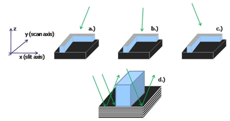
Mask Shadowing is truly unique to EUV lithography. Because everything (all solids, liquids, and gasses anyway) absorb 13.5nm EUV wavelength, EUV exposure tools must use mirrors for all optical elements and for the mask. Unlike the telecentric refractive projection lens systems used in optical lithography, EUV systems rely on off-axis mask illumination. Currently, the angle of incidence is 6o from normal. Even more problematic is the complication of the azimuthal angle. This angle varies across the scanner’s illumination slit and ranges from 0o to +/- 22o [2].
Off-axis mask illumination wouldn’t be a problem if we lived in a perfect world where the mask has no topography, and is infinitely thin. But unfortunately, the mask absorber has thickness, and the mask reflector is a distributed Bragg reflector composed of alternating thin-film layers. Thus, off-axis mask illumination results in an uneven shadowed reflection depending on the orientation of the mask shapes and the angle of incidence. This is shown in the figure below.

Figure : Mask topography and azimuthal angles for left (a), center (b), and right (c) region of the scan slit. Detailed view (d) showing how the mask in the right region of the scan slit will shadow both incoming light from the source, and light reflected from the mask substrate.
The result is an orientation-dependent pattern bias and shift, which is also a function of the location within the scanner slit. Current estimates of the magnitude of this effect range from 1-2nm for longer lines, and >5nm for small 2D shapes like contact & via holes. Variation in wafer CDs of this magnitude are obviously unacceptable.
Compensating for Mask Shadowing Effect requires new 3D mask topography models. Existing TCAD lithography simulators can already accurately predict the effects but cannot be directly adapted for use in OPC due to their very long simulation times. These models were designed to be very, very fast under certain assumptions: a thin mask with no topography (the Kirchhoff approximation), and a normal illumination incidence at the mask plane. Neither is valid in EUV exposure tools. The EDA industry has already introduced fast 3D mask topography models capable of simulating an entire chip with minor runtime penalty and with an accuracy approaching that of TCAD simulators. New OPC models that correctly handle off-axis incidence at the mask plane are becoming available.
However, we won’t be able to accurately model the mask shadowing effects until the software can handle the fact that the angle of illumination incidence is now a function of the location within the scanner field, as shown in Figure 1. The best solution now may be a hybrid of rules and model-based mask shadow compensation: models to handle the field-location-invariant component, with rules to compensate for the field-dependent component.
Conclusion
The upcoming availability of EUV scanners will enable further technology scaling. Initially, the features being imaged by EUV scanners will be larger than the 13.5nm illumination wavelength, and this would seem to provide some breathing room to the over-worked OPC engineers of the world. But as we’ve demonstrated here, the unique illumination source, reflective optics, and reflective masks are conspiring to ensure continued full employment amongst these engineers. So I think we can safely predict there will be no OPC engineer’s holiday for the foreseeable future.
–James Word, OPC product manager at Mentor Graphics.
Share this post via:


Comments
0 Replies to “With EUVL, Expect No Holiday”
You must register or log in to view/post comments.