In part I of this series, we looked at the history of lithography process models, starting in 1976. Some technologies born in that era, like the Concorde and the space shuttle, came to the end of their roads. Others did indeed grow and develop, such as the technologies for mobile computing and home entertainment. And lithography process models continue to enable sub-wavelength patterning beyond anyone’s imagination a few years ago. As for the lasting impact of Barry Manilow, well, you can’t argue with genius. But back to lithography process models. Here’s a summary timeline of process model development:
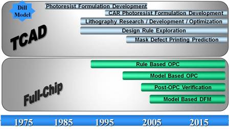
In this second part in the series, I want to talk even more about the models themselves. The next parts will address requirements like accuracy, calibration, and runtime, as well as the emerging issues. I particularly appreciate the reader comments on Part I, and will attempt to address them all. [Yes, I take requests!]
Recall that TCAD tools are restricted to relatively small layout areas. Full-chip, model-based OPC can process several orders of magnitude more in layout area, partly because of a reduction in problem dimensionality. A single Z plane 2D contour is sufficient to represent the relevant proximity effect for full-chip OPC. Some of the predictive power of TCAD simulation is not relevant for OPC given that the patterning process must be static in manufacturing as successive designs are built.
There are domains of variability where a model needs to dynamically predict, but these are largely limited to errors in mask dimension, dose, focus, and overlay. Dose can serve as a proxy for a variety of different manufacturing process excursions, such as PEB time and temperature. Some mathematical facets of these photoresist chemistry, such as acid-based neutralization or diffusion, can be incorporated into process models, but useful simulation results do not depend on a detailed mechanistic chemical and kinetic understanding. The information that would come from such mechanistic models is very useful for process development, but not strictly necessary for OPC in manufacturing.
Optical models for a single plane did not require dramatic simplification from TCAD to OPC, but the photoresist and etch process models used in full-chip OPC are fundamentally different. Starting with the Cobb threshold approach, these photoresist and etch process models models are variously referred to as semi-empirical, black box, compact, phenomenological, lumped, or behavioral. Whatever you call them, they are characterized by a mathematical formulation that provides a transfer function between known system inputs and measured outputs of interest. Notably, the user does not need access to sophisticated physiochemical characterization methods. Rather, all the inputs required for the model are readily available in the fab.
Photoresist Models
There are two basic types of photoresist process models used in full chip simulations; those that threshold the aerial image in some manner, and those that transform the aerial image shape. Alternatively, the model types could be parsed by variable or constant threshold. Earlier full-chip models were based upon the aerial image cutline of intensity versus position, with the simplest form a constant threshold. Accuracy increased by defining the threshold as a polynomial in various simulated image properties associated with the aerial intensity profile, as shown in Figure 1. Initially Imin and Imax were utilized, then image slope was added, then image intensity at neighboring sites, and finally a variety of functions used to calculate pattern density surrounding the site under consideration. Thus multiple different modelforms are possible.
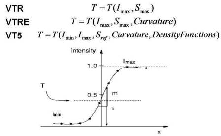
Figure 1. Variable Threshold resist models schematic.
More recent full-chip simulation (“dense” simulation, which I’ll discuss in another part of this series) was accompanied by a new type of resist model (CM1) that applied a constant threshold to a two dimensional resist surface. The resist surface is generated by applying a variety of fast mathematical operators to the aerial image surface. These operators include neutralization, differentiation of order k, power n, kernel convolution, and n order root. This is expressed in the equation below:

The user can specify a modelform that selects which operators and k, n, and p values are desired, thus as with the above variable threshold model, a huge number of different forms are possible. The linear coefficients Ci and continuous parameters b and s are found by minimizing the objective function during calibration.
A nominal exposure condition model fit result is shown in Figure 2, which compares a constant threshold aerial image result with a CM1 model fit for 1D features, Figure 3, which does the same for 2D features, and Figure 4, which shows overall CM1 model fitness for 695 gauges.
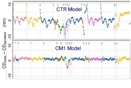
Figure 2: CM1 modelfit for 1D structures.
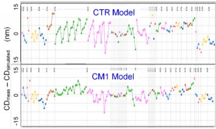
Figure 3. CM1 modelfit for 2D structures.
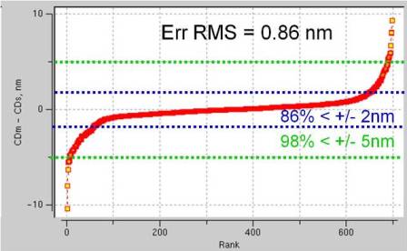
Figure 4. CM1 modelfit for all structures (695 gauges).
It is interesting to note that the accuracy of OPC models has roughly scaled with the critical dimensions: an early paper by Conrad et al. on a 250 nm process reported errors of 17 nm 3σ for nominal and 40 nm 3σ for defocus models. The model accuracy for today’s 22 nm processes is on the order of 10X lower than these values. Typical through process window results are shown in Figure 5. It can be seen that CDerrRMS of 1 nm is achieved and the errRMS value is maintained below 2.5 nm throughout the defined focus and dose window.
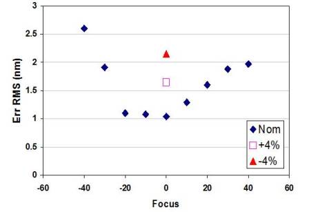
Figure 5. Example results for CM1 model fitness at different focus and three exposure dose conditions. Comparable accuracy to TCAD models.
Etch proximity effects are known to operate locally (i.e. on a scale similar to those of “optical” proximity effects) as well as over longer distances; approaching mm scale. Long distance loading effects can be accounted for but typically result in long simulation runtimes, whereas the shorter range effects can be compensated effectively. The two primary phenomena are aspect ratio dependent etch rates (ARDE), and microloading. With ARDE, the etch rate and therefore bias is seen to depend upon the space being etched, while microloading dictates that the etch bias is dependent upon the density of resist pattern within a region of interest. Different kernel types can accurately represent these phenomena, capturing the local pattern density and the line of sight visible pattern density. When used in combination, these variable etch bias (VEB) models can yield a very accurate representation of the etch bias as a function of feature type, as show in Figure 6.
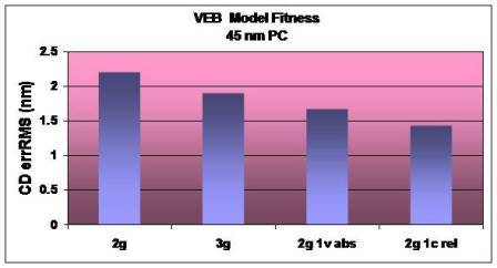
Figure 6. Example VEB model fitness for a 45 nm poly layer. Model error for four different types of kernel combinations: 2 gauss kernels, 3 gauss kernels, 2 gauss and 1 visible kernel, 2 gauss and 1 visible kernel.
So there you have the two main OPC model types. Next I’ll talk about how they actually work in practice, including the concepts of sparse vs. dense simulation and how the OPC software addresses the principal accuracy and predictability, ease of calibration, and runtime.
OPC Model Accuracy and Predictability – Evolution of Lithography Process Models, Part III
Mask and Optical Models–Evolution of Lithography Process Models, Part IV
John Sturtevant, Mentor Graphics
Share this post via:


Comments
There are no comments yet.
You must register or log in to view/post comments.