
Chiplet is a hot topic in the semiconductor world these days. So much so that if one hasn’t heard that term, the person must be living on a very isolated islet. Humor aside, products built using chiplets-based methodology have been in existence for at least some years now. Companies such as Intel, AMD, Apple and others have integrated in-house chiplets to build these products. But the bigger opportunity lies in being able to build products using heterogeneous chiplets, meaning chiplets from multiple vendors. Heterogeneous chiplets integration poses many technical and business challenges to overcome.
The Open Compute Project Foundation has a subgroup called Chiplet Design Exchange (CDX) that is now focused on tackling the technical challenges. The effort is a collaborative one with Palo Alto Electron, Siemens EDA and many other companies and individuals participating and contributing. Jawad Nasrullah, CEO of Palo Alto Electron gave a talk at Siemens EDA’s User2User conference in Santa Clara, CA. The following are excerpts from that presentation.
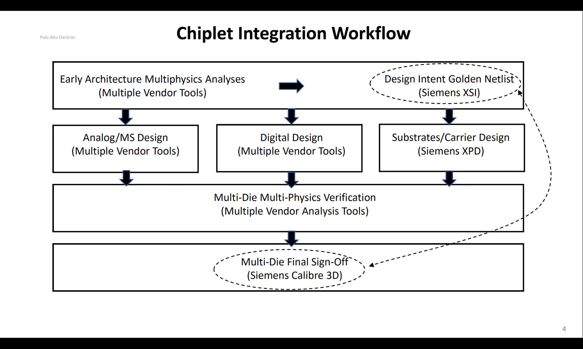
Design management of chiplet projects can be broadly divided into four stages, namely architecture, design execution, verification and signoff.

The architecture stage needs to consider multiphysics including thermal, warpage, structure, etc., on top of the conventional power, performance and area (PPA) metrics. The goal is to generate a top level golden netlist based on all of the above considerations. Even a simple design could have tens of thousands of nets and typical designs could have nets in the millions. The Open Compute Project/ODSA subgroup is happy with the capabilities of Siemens EDA’s XSI tool for managing the golden netlist.
Design automation and management become very critical in a multi-vendor tools environment. In dealing with substrates for chiplets-based designs, bridges, interposers, etc. make things more complicated. A standardized workflow is needed to tackle the many challenges. Siemens EDA’s XPD solution does a pretty good job although there is room for improvement. Current tools in the market fall short a bit as they are being repurposed from their PCB oriented purpose to support packaging for chiplet-based designs. Participants and contributors to the CDX subgroup project are using Siemens Calibre 3D for signoff related R&D, making it easier to use the Siemens XSI generated golden netlist.
 Charter")
The above is the foundation for the work being done in CDX, with the goal of design automation standardization. In order for EDA tools from multiple vendors to be able to exchange design information, models need to be standardized and described in machine readable format.
The goal of CDXML is to provide a standardized format for describing chiplets, which will enable chiplets from different vendors to be easily integrated into a single system-on-chip (SoC) design. CDXML is designed to be compatible with existing Electronic Design Automation (EDA) tools and workflows, which are used to create and verify chiplet-based designs. Once the chiplets are defined, they need to be modeled to capture their thermal, physical, mechanical, I/O, behavioral, power dissipation, signal integrity, power integrity and testability aspects. A chiplet design kit (CDK) is a collection of tools, models and documentation that enable designers to create and verify complex chiplets-based SoCs. CDKs are to be provided by chiplet vendors in a heterogeneous chiplets market place.
CDX subgroup participants including Palo Alto Electron and Siemens EDA have contributed to a proposed standardization effort for chiplets modeling for heterogeneous integration.
You can download the whitepaper here. Those involved in chiplets-based designs currently or will be in the future will find this whitepaper very useful.
Also Read:
Chiplet Q&A with Henry Sheng of Synopsys
Anirudh Keynote at Cadence Live
Share this post via:


Comments
There are no comments yet.
You must register or log in to view/post comments.