Recently, TSMC held their 26th annual Technology Symposium, which was conducted virtually for the first time. This article is the last of three that attempts to summarize the highlights of the presentations. This article focuses on the technology design enablement roadmap, as described by Cliff Hou, SVP, R&D.
Key Takeaways
- Design enablement is available for N7, N6, N5, and N3, both EDA reference flows and Foundation IP.
- N3 “specialty” IP is in development, in collaboration with the IP Partners.
- Automotive (AEC-Q100) Grade 1 qualification is progressing for N7, offering an attractive PPA migration from N16 (available 4Q20).
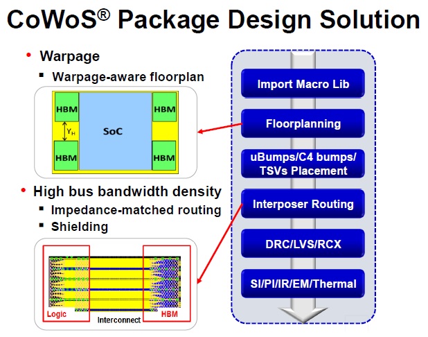
- EDA tool support is available for leading 2.5D/3D package technologies: SoIC, InFO, CoWoS. New EDA flow support required for (>1X reticle size) packages will be available 4Q20 (e.g., package warpage analysis).
Introduction

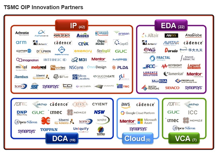
It is no secret that a major factor in TSMC’s foundry success has been the investment in the design enablement ecosystem, which spans the collaboration between TSMC and:
EDA partners
- enhancing tool algorithms for new process node requirements, from place-and-route to physical design layout verification
- collaborating with TSMC on implementation of trailblazing designs, from process bring-up memory array testsites to advanced Arm cores
- preparing an integrated (and qualified) “reference flow” for a new process node
IP providers
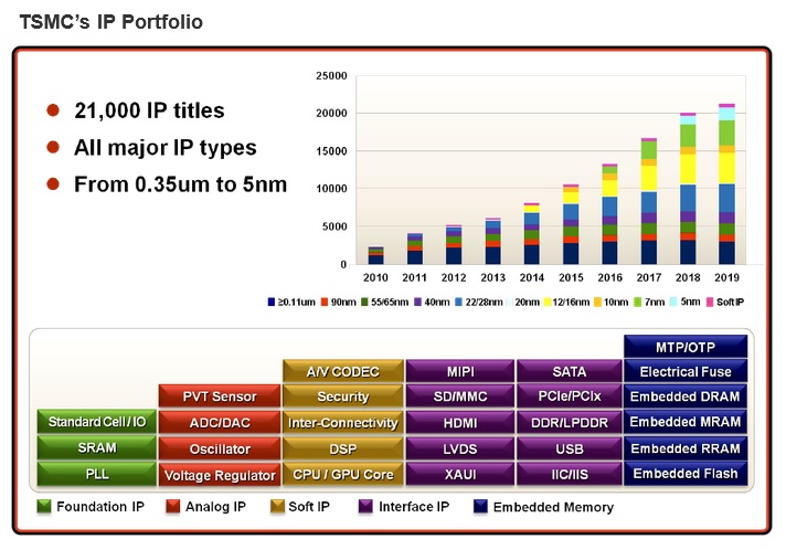
- developing critical IP functionality in a new node to complement TSMC’s Foundation IP
- qualifying test silicon in the new node for the various TSMC platforms – IoT, mobile, HPC, and (the most demanding) automotive

Design Center Alliance (DCA) service providers
- offering a range of front-end design resources, back-end implementation skills, custom design support, and DFT services
Value Chain Aggregator (VCA) providers
- offering a broad range of support, throughout the IC “value chain”, extending all the way from product architecture definition to final wafer assembly/test/qualification services
and, the most recent addition to the Open Innovation Platform (OIP) ecosystem,
Cloud Alliance partners
- collaborates with TSMC and EDA partners to provide a secure, scalable cloud compute environment for some (i.e., burst demand) or all of the IC design flow
The heart of the Open Innovation Platform is the TSMC Design Enablement (DE) organization. Cliff provided an update on the enablement status for the upcoming advanced process nodes and packaging technologies, across the various design platforms.
Tool Certification
It should be noted that EDA tool certification at a new node is far more complex than simply running a set of SPICE circuit simulations and updating the runsets used for DRC/LVS/ERC physical verification. Each node transition commonly introduces new, complex layout design rules, often requiring significant algorithm development by the EDA partner to provide the functionality and language commands needed to code the runset. Multi-patterning, forbidden pitches, run-length dependent rules, line cut rules, and specific fill requirements across multiple mask levels all have been introduced at recent nodes. For block composition flows at successive nodes, each cell library may have rules that define new constraints on cell placement, pin access routing, and power distribution/gating. Reaching tool/flow production certification is no mean feat.
Additionally, new process nodes (and their application markets) may necessitate the introduction of completely new flows:
- an “aging flow” that integrated the effects of NBTI, PBTI, and HCI into a measure of performance degradation over time, using new device aging models
- a local heating flow that reflects how the unique thermal dissipation paths in FinFET-based designs impact chip failure mechanisms (especially electromigration)
N7/N6/N5/N3
- full EDA tool certification, for both custom IP design and cell-based block composition, for all nodes (N5: v0.9 PDK; N3: v0.1 PDK)
- EDA “utility” certification (e.g., fill algorithms)
(Cliff’s certification charts focus on tool offerings from the major EDA Partners.)
N6 is a variant of N7, offering a yield improvement (fewer mask layers) and the ability to achieve a logic block density improvement using an optimized N6 high-density cell library.
- N7 automotive platform flows and IP ready (AEC-Q100 Grade 1)
- N5 automotive platform in 2022 (Grade 1)
Note that there are two common reliability qualification designations for the AEC-Q100 automotive platform, both based on zero fails after 1K hours HTOL stress test on sampled lots, plus HAST and temperature cycling endurance tests: Grade 1: -40C to 125C; Grade 0: -40C to 150C (for “under the hood” applications).
When describing the (Grade 1) qualification activity for N7 and N5, Cliff highlighted some of the additional design enablement considerations for the automotive platform:
- a “low DPPM” Design Rule Manual and DRC runset
- aging model qualified for the automotive part lifetime and operating temperature
- automotive platform-specific EM rules
- automotive platform-specific latchup and ESD design rules
- soft error upset analysis
Since the automotive “defect parts per million” shipped criterion is stringent, a specific set of DRC rules at the node is employed.
The demand for high-throughput, low power computation in the vehicles of the future is great , and must also meet the AEC-Q100 qualification criteria (Grade 1). The TSMC design enablement team is extending the technology definition, design rules, models, and Foundation IP evaluation to provide this support at advanced process nodes.
N12e
At the Symposium, TSMC introduced a new ultra low power N12FFC+ variant, denoted as N12e. This process is specifically designed for IoT (and AIoT, or AI at the edge) applications, offering a transition from N22ULL (planar) to N12e (FinFET).
- N12e EDA tools certified (major new features added, listed below)
The design enablement for N12e is faced with the challenges of:
- analyzing and modeling layout dependent effects (LDE), where device impacts are magnified at low VDD
- developing SPICE models valid for VDD=0.4V
- providing statistical device model support valid for low VDD operation
- providing cell characterization, delay calculation, and static timing analysis support valid for low VDD operation; specific focus is required for flip-flop setup/hold measures at low VDD
(At low supply voltage, the cell delay arc statistical variation is decidedly non-Gaussian, due to the “near Vt” operation.)
Advanced Packaging: SoIC, InFO, CoWoS (3D Fabric)
With the rapid growth of 2.5D and 3D packaging options, the TSMC Design Enablement team has expanded their scope to include the appropriate physical verification and electrical/thermal analysis EDA flow support:
- redistribution Layer (RDL) routing and through via routing rules (through CoWoS silicon interposer or InFO wafer compound)
- routed interconnect impedance matching and shielding requirement (e.g., on a CoWoS interposer, to support wide bus width connectivity to HBM stacks)
- die-to-die bond rules (SoIC)
- LVS verification throughout the 2.5D/3D package connectivity
- RC and RLC parasitic extraction for a complex package geometry – especially, inter-die coupling capacitance for SoIC
- IR and EM analysis of the power distribution network throughout the package assembly
- signal integrity analysis
- thermal analysis – especially, through 3D stacked die
- ESD analysis
EDA tools are ready for SoIC (3D), InFO and CoWoS (both 2.5D), with the following exceptions, as new flows need to be certified:

- large (>>1X max reticle size) multi-die floorplan package “warpage analysis” (available for InFO and CoWoS in 4Q20)
- static timing analysis for stacked die in an SoIC, with temperature/voltage distribution and “multi-corner” process variation between die (available 4Q20)
The TSMC Design Enablement team continues to provide EDA tool and reference flow support for the challenges introduced by advanced process nodes, ranging from new aging models to timing/electrical analysis at low VDD operation. The 2.5D and 3D package technology offerings require a close collaboration between TSMC and EDA developers to address new requirements – e.g., unique package interconnect/via design rules, stacked die timing analysis.
As mentioned above, TSMC’s focus on design enablement distinguishes their process and package technology offerings.
For more information on the TSMC Design Enablement support for the OIP Partners and platforms, please follow these links – OIP and Technology Platforms.
-chipguy
Highlights of the TSMC Technology Symposium – Part 1
Highlights of the TSMC Technology Symposium – Part 2
Share this post via:


Comments
There are no comments yet.
You must register or log in to view/post comments.