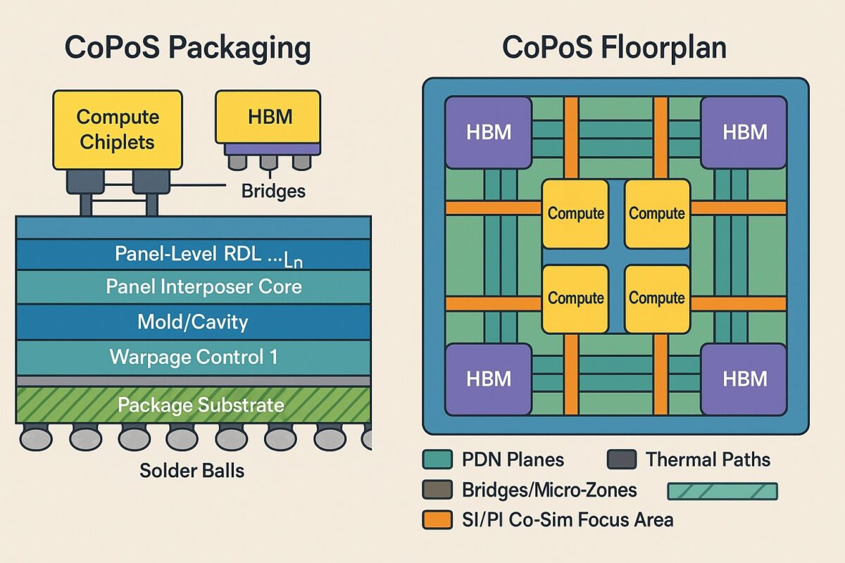
Chip on Panel on Substrate, often shortened to CoPoS, extends the familiar idea of chip on carrier packaging by moving the redistribution and interposer style structures from circular wafers to large rectangular panels. The finished panel assembly is then mounted on an organic or glass package substrate. This shift from round to rectangular carriers is much more than a cosmetic change. It is a deliberate move toward greater area, better utilization, and higher throughput, all aimed at the rapidly growing needs of artificial intelligence and high performance computing where packages must host many chiplets and numerous stacks of high bandwidth memory.
A typical CoPoS module begins with compute chiplets and memory stacks placed above a panel level interconnect fabric. That fabric may be a redistribution layer on an organic or glass core, or a fan out style build up formed directly on the panel. Designers can also add small silicon or organic bridges only in the local regions that demand the very finest routing. After interconnect formation, the panelized assembly is bonded to a high density package substrate and completed with underfill, mold, warpage control layers, and external solder balls for board attachment. There are several process styles. In a chip first flow, dice are placed on the panel carrier before the redistribution layers are patterned. In a chip last flow, the redistribution structure is created first and dice are attached afterward. Hybrid flows use bridges only where essential to reach line and space under ten micrometers.
The economic appeal comes from geometry and logistics. Rectangular panels waste less material at the edges and can hold more large modules than a circular wafer. Exposure and handling steps can be tuned for panel throughput, which lifts overall productivity. Even more important, the architecture lets teams reserve expensive silicon only for small high density islands while most long routes use lower cost organic or glass wiring. That mix and match approach opens floorplanning freedom. Compute islands and memory can be placed for performance first, and only the hotspots that need extreme bandwidth receive the densest treatment.
Scale also magnifies challenges. Power delivery becomes the primary constraint, since hundreds or even thousands of amps must cross a very large structure with minimal inductance. Successful projects start with the power delivery network, including wide planes, via fields, decoupling placement, and return path continuity. Signal integrity follows closely. Long routes across a panel require careful impedance control, timing and skew management, and disciplined reference plane design. Glass cores help by offering flatness and stable dielectric properties, while advanced organic systems continue to improve.
Thermal design is equally central. Multiple hot chiplets and tall memory stacks create non uniform heat maps that can degrade reliability and performance if ignored. Teams rely on heat spreaders, vapor chambers, tuned interface materials, and carefully placed keepout corridors that preserve airflow and mechanical attachment for the cooling solution. Thermal and electrical analysis must be run in tandem because each choice influences the other.
Mechanical reliability adds another layer of complexity. Materials across the stack expand at different rates with temperature. That difference causes warpage and die shift during cure and reflow. Symmetric stacks, staged cures, low stress resins, and local stiffeners are practical tools for control. At the board level, very large packages place high strain on solder joints. Corner keepouts, dummy copper, and under package stiffening can extend life significantly. Test strategy must adapt as well. Known good die becomes non negotiable, at panel coupons and daisy chains validate redistribution before singulation, and boundary scan or built in self test features allow rapid screening of huge input and output counts.
Design enablement ties the story together. The panel interposer is not just a mechanical support. It is an electrically significant substrate that must be co simulated with the dice and the board for power and signal behavior. Early floorplanning guided by power maps and thermal models prevents late surprises. Design for manufacturability is a front end activity. Overlay budgets, expected die shift, and warpage envelopes all drive guard bands and alignment rules that belong in the kit, not in the lab notebook.
CoPoS fits best where systems demand many chiplets, abundant memory, and package level bandwidth that rivals on die fabrics. It does not eliminate silicon interposers. Instead it uses them surgically while the panel fabric provides scale. As panel tools, glass cores, and large field imaging continue to mature, CoPoS makes very large and very capable packages practical, and brings the substrate directly into the performance roadmap.
Also Read:
PDF Solutions and the Value of Fearless Creativity
Streamlining Functional Verification for Multi-Die and Chiplet Designs
Enabling the Ecosystem for True Heterogeneous 3D IC Designs
Share this post via:


Musk’s Orbital Compute Vision: TERAFAB and the End of the Terrestrial Data Center