
In a major announcement at the 2025 Design Automation Conference (DAC), Siemens EDA introduced a significant expansion to its electronic design automation (EDA) portfolio, aimed at transforming how engineers design, validate, and manage the complexity of next-generation three-dimensional integrated circuits (3D ICs). With the launch of the Innovator3D IC solution suite and Calibre 3DStress, Siemens EDA delivers an end-to-end, multiphysics-driven environment aimed at tackling the inherent challenges of heterogeneous, multi-die integration.
I chatted with Keith Felton, Principal Technical Product Manager for Siemens EDA’s semiconductor packaging solutions, and Shetha Nolke, Principal Product Manager for its Calibre 3DStress tool, to gain additional insights.
3D ICs and the Need for Coherent Design Platforms
As the semiconductor industry increasingly pivots toward chiplet-based and 3D packaging architectures, traditional tools for physical design, thermal analysis, and data management are proving insufficient. The benefits of 3D ICs—ranging from higher performance and energy efficiency to reduced footprint and modular reuse—come with trade-offs in integration complexity and packaging-induced reliability challenges.
Siemens EDA’s newly introduced technologies aim to provide a unified, scalable solution to this new design paradigm. By embedding intelligent simulation, AI-powered layout assistance, and full-stack thermal-mechanical analysis, the company seeks to remove major roadblocks that have traditionally hampered development of these advanced systems.
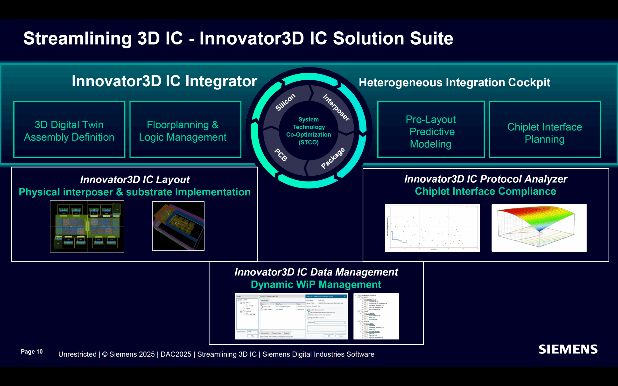
Innovator3D IC: A Unified Platform for 3D System Design
At the core of Siemens EDA’s announcement is the Innovator3D IC, a modular suite purpose-built for design teams developing heterogeneously integrated 2.5D and 3D chip architectures. Unlike traditional EDA tools that treat multi-die systems as loosely connected components, Innovator3D IC provides a centralized, coherent framework that enables comprehensive design authoring, system-level simulation, and rigorous interface management.

The suite is anchored by Integrator, a cockpit that allows designers to visualize and configure all physical, electrical and thermal characteristics of a 3D IC system stack. With Integrator, engineering teams can manage die-to-die placement, define vertical interconnects, and simulate package-aware system behavior within a single interactive workspace. This enables faster iteration and earlier identification of system bottlenecks.

Complementing this is the Layout Solution, a correct-by-construction environment purpose-built for interposer design and silicon bridge planning. This tool enables designers to author highly constrained routing between chiplets and substrates while respecting package-level constraints and thermal zones.
Another key component is the Protocol Analyzer, which ensures high-speed chip-to-chip interfaces conform to expected protocol standards and signal integrity thresholds. It plays a critical role in verifying that chiplet communication pathways meet stringent electrical and timing requirements early in the design phase.
Finally, the suite includes a robust Data Management layer, which consolidates all relevant design metadata, IP reuse information, and interface specifications. This unified data model supports traceability and revision control across multi-team projects, reducing errors and accelerating design closure.
What distinguishes Innovator3D IC from legacy tools is its scalability and performance. Built with advanced multithreading and powered by AI-assisted layout guidance, the suite can efficiently handle designs featuring over five million pins—meeting the demands of the most complex AI, mobile, and high-performance computing (HPC) architectures.
Calibre 3DStress: Predictive Reliability at the Transistor Level
To complement its Innovator3D IC suite, Siemens EDA also introduced Calibre 3DStress, a first-of-its-kind tool that brings transistor-level resolution to thermo-mechanical analysis. Unlike traditional stress modeling tools that evaluate packaging effects at a die-level scale, Calibre 3DStress provides granular insights into how physical stresses impact individual transistors and circuit blocks.

This capability is essential in modern 3D ICs, where materials with differing coefficients of thermal expansion—across dies, interposers, and substrates—can induce localized strain during manufacturing and operation. These stress-induced deformations can subtly alter transistor behavior, shift threshold voltages, and compromise timing margins, ultimately threatening circuit-level performance even if all nominal design rules are met.
Calibre 3DStress allows engineering teams to simulate such effects with high fidelity before a single chip is fabricated. By modeling post-reflow and operational mechanical stresses and correlating them with electrical performance metrics, the tool enables designers to verify that neither the packaging process nor the final use environment will degrade circuit behavior or long-term product reliability. This simulation engine is fully integrated with Siemens EDA’s existing Calibre 3DThermal technology, allowing for comprehensive multiphysics analysis that spans thermal profiles, structural deformation, and transistor behavior within a unified verification flow.

Positioned for the Future of System Design
Together, Innovator3D IC and Calibre 3DStress represent a strategic leap for Siemens EDA and its customers. These solutions realign the entire development process around the realities of modern system integration. As semiconductor companies embrace chiplet reuse, heterogeneous architectures, and rapid design cycles, the ability to plan, simulate, and verify at scale will be critical. By combining intelligent design orchestration with predictive, physics-based verification, Siemens EDA has positioned itself as a catalyst for the next wave of semiconductor innovation.
To learn more about Siemens EDA’s broad portfolio of solutions for 3D IC architectures, visit here.
Also Read:
Jitter: The Overlooked PDN Quality Metric
DAC News – A New Era of Electronic Design Begins with Siemens EDA AI
Share this post via:


Comments
There are no comments yet.
You must register or log in to view/post comments.