
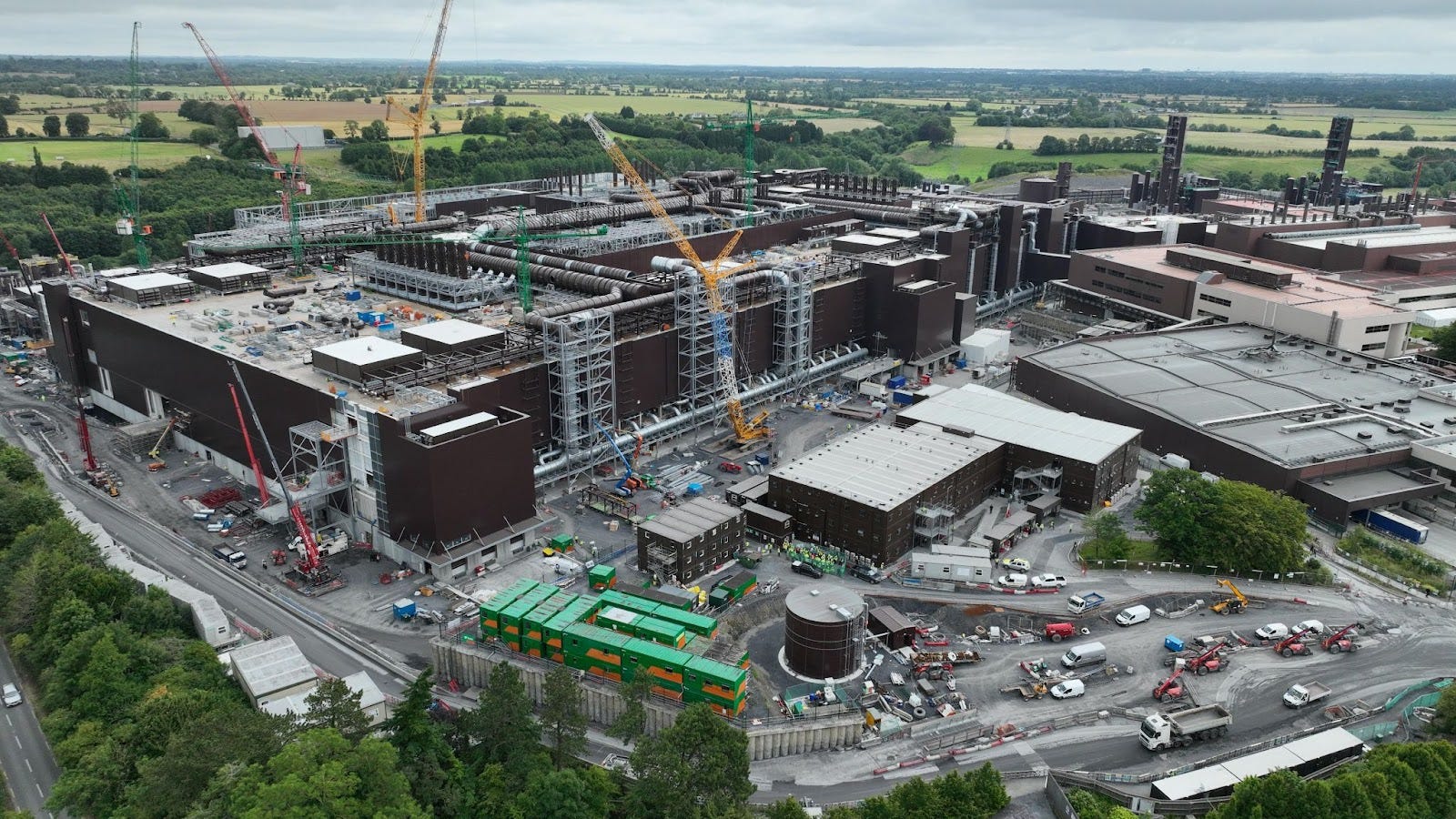
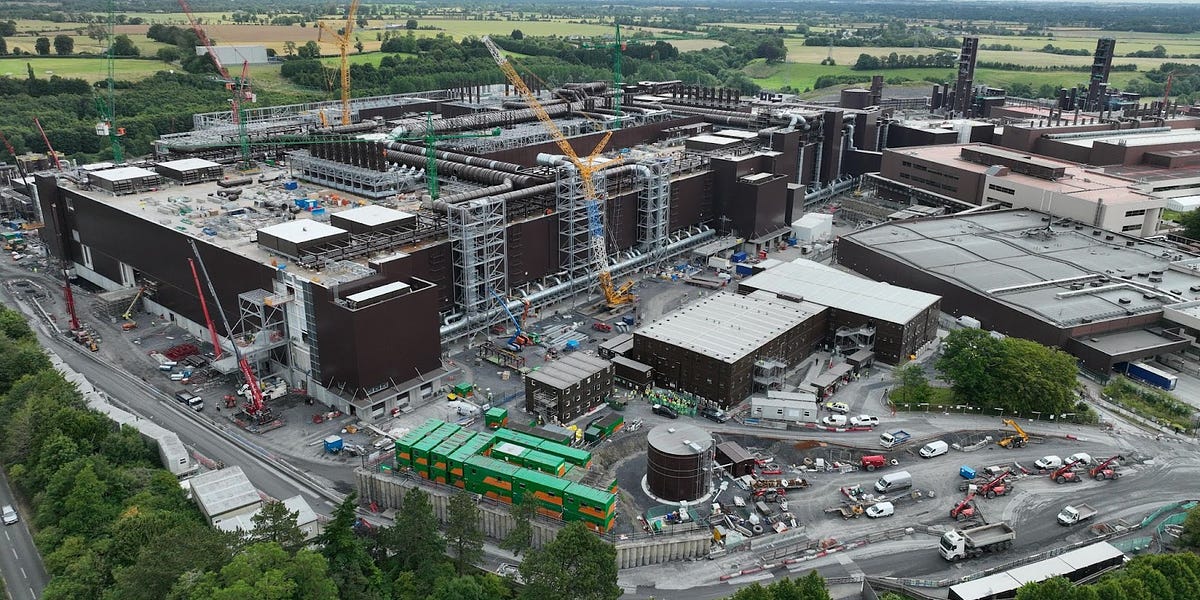
Intel fab under construction in Ireland, via Intel Ireland
For the last several decades, one avenue of technological progress has towered over nearly everything else: semiconductors. Semiconductors are materials that can have their conductivity varied by many orders of magnitude, which makes it possible to selectively block and allow the flow of electrons. This property makes it possible to manufacture all sorts of electronic devices, not least of which is the digital computer.
As semiconductor technology has advanced over the past several decades, the cost and size of electronic computation has steadily fallen, making the PC, the internet, and mobile phones all possible. Today, semiconductors in the form of powerful GPUs that can perform enormous numbers of matrix multiplications are the keystone for advancing AI technology. Increasingly available computation to do enormous amounts of search and learning drives progress in things like game-playing AI, computer vision, and large language models (LLMs).
As Moore’s Law has marched forward, transistors (an electronic switch which is the fundamental building block of integrated circuits) have gotten smaller and cheaper. In 1954, the first transistor radio, the TR-1 had 4 transistors which cost $2.50 apiece ($29.03 in 2024 dollars). Today, an AMD Ryzen processor with 9.9 billion transistors is on sale for $650, or about $0.000000066 per transistor; in other words, since the 1950s the cost of a transistor has fallen by about a factor of 300 million.
The same shrinking and cheapening has happened for every semiconductor component. But at the same time, the facilities to manufacture them have become increasingly expensive. In the late 60s and early 70s, a semiconductor fabrication facility (or ‘fab’) cost on the order of $4 million (~$31 million in 2024 dollars). Today, a modern fab can cost $10-$20 billion or more. Intel is building a pair of fabs in Arizona which are projected to cost $15 billion apiece, and Samsung’s fab in Taylor, Texas is projected to cost $25 billion.
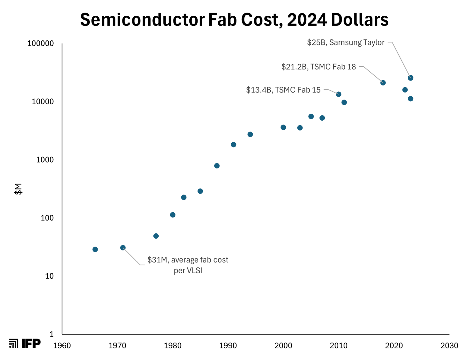
These enormous costs are ultimately due to the same factor that has steadily driven down the cost of semiconductors: Moore’s Law, the observation that the number of components on an integrated circuit tends to double every two years. (There is a Moore’s Second Law, also known as Rock’s Law, which posits that the cost of a semiconductor fab doubles every four years.) The smaller semiconductor components get, the more difficult it is to create the conditions to manufacture them.
A modern microchip has features on the order of 50 nanometers in width, or around 1/2000th the width of a human hair.1 Materials are placed in layers a few atoms thin. Creating objects this small requires ultra-precise manufacturing equipment, and a production environment that can screen out as many sources of interference as possible; every rogue speck of dust or tiny fluctuation in electrical voltage. And these conditions must be maintained not in the rarefied conditions of an experimental lab, but in a mass production facility that is producing hundreds of millions of microchips every year. The combination of ultra-precision and high-volume production results in some of the most complex, expensive factories in the world.
The semiconductor fabrication process
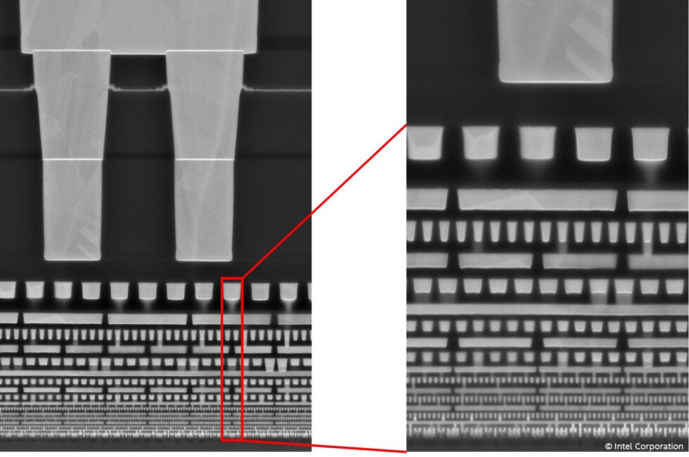
To understand why a modern fab is so expensive, we first need to understand the process for manufacturing semiconductors.If we sliced a computer chip down the middle, and looked very, very closely, we would see that it is composed of a series of layers. Here is a cross section of a chip made with Intel’s current manufacturing process:
And here’s an illustrated cross section of a generic integrated circuit, showing the different layers:
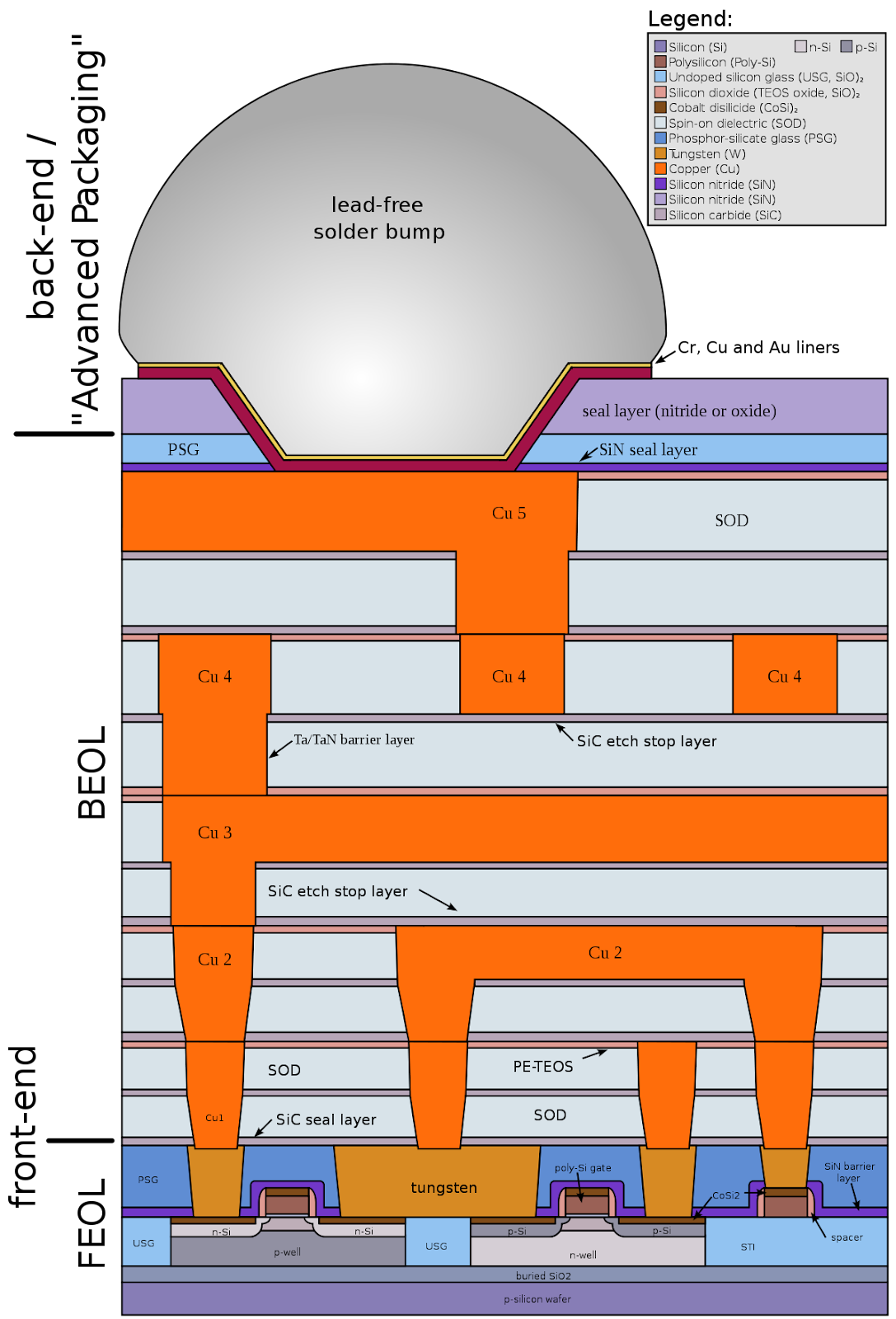
Via Wikipedia.
At the bottom of the chip, the area marked FEOL (front end of line) on the graphic above are the semiconductor components themselves: transistors, capacitors, resistors, diodes, and all the other parts created out of silicon to make a microchip.2 These individual components will be connected together using microscopic metal wires, the layers in the area marked BEOL (back end of line). Because of the enormous number of components in a modern electronic chip, this wiring must be routed on separate layers, which are separated by electrical insulators known as dielectrics. Intel’s current process, for instance, consists of 15 layers of metal wiring. This wiring gets connected together and to the semiconductor components through holes in the layers known as ‘vias.’
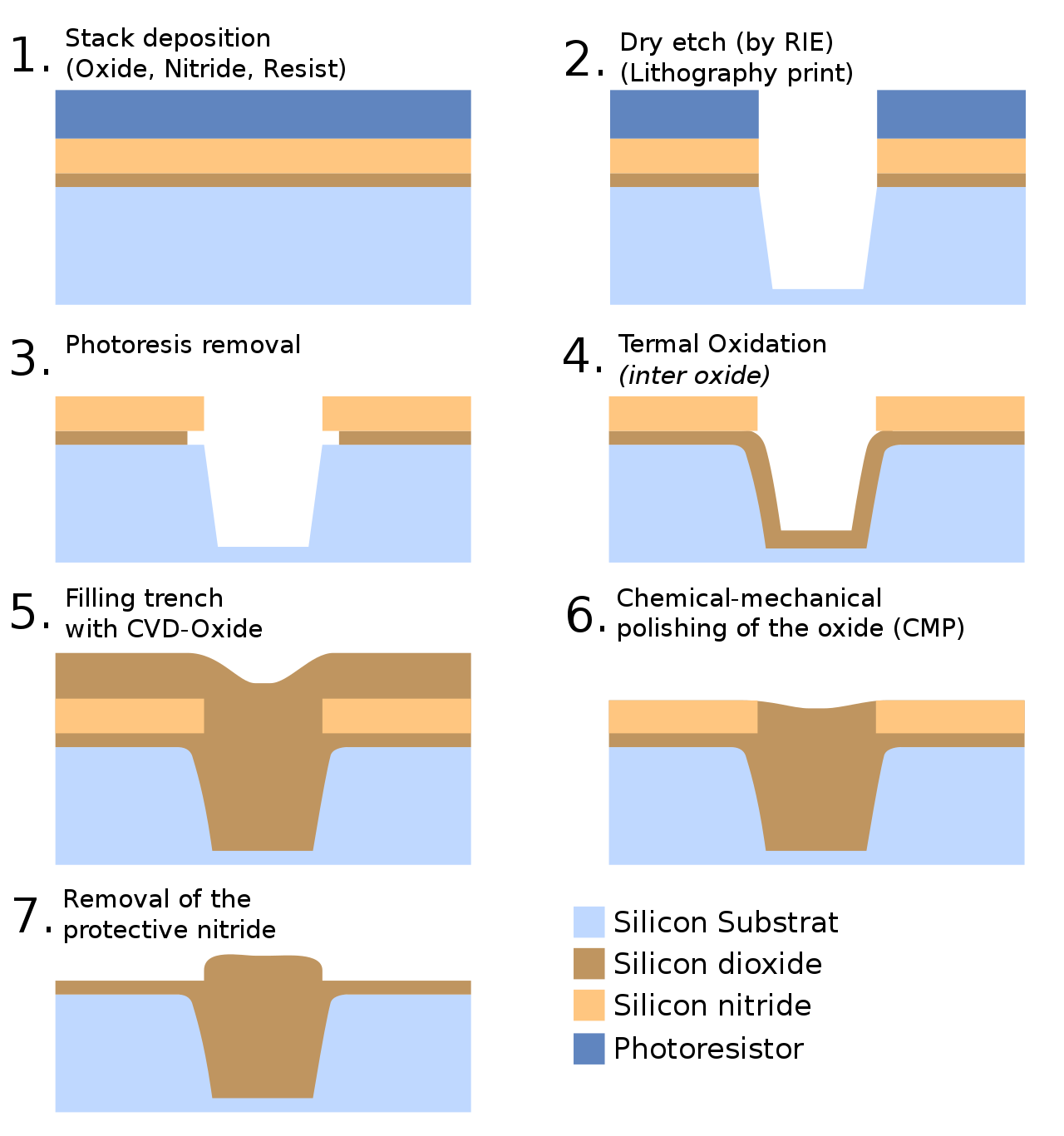
Chips are made by building up this complex structure one layer at a time. Starting with a wafer of extremely pure silicon, layers of material are added, portions of the layer are removed, more material is added (or existing material is modified), and so on, until the entire structure is complete. This fabrication method is known as the planar process, and it was invented at Fairchild Semiconductor in 1959 by Jean Hoerni. It’s what makes integrated circuits, and modern computer technology, possible.
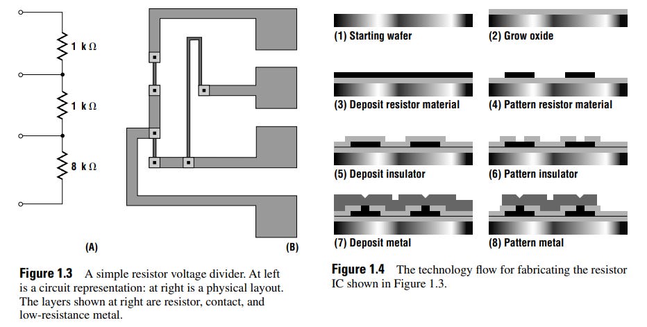
A simple electronic voltage divider and the fabrication steps to produce it. Via Fabrication Engineering at the Micro- and Nanoscale
The process for building up the structure of a microchip can be broken down into four basic operations, repeatedly applied: layering, patterning, doping, and heat-treating.
Layering
Layering is used to add an extremely thin layer of material — as little as a nanometer or less, 1/100,000th the thickness of a human hair — to the surface of the wafer. These layers might be insulators (such as layers of silicon dioxide used to separate components), conductors (such as layers of copper wiring used to connect components) or semiconductors (such as epitaxial thin films of silicon which form part of the semiconductor components). Depending on the step in the process and the material being used, different layering techniques might be applied.Deposition methods have also evolved over time as features have shrunk. Current common layering methods include thermal oxidation (exposing wafers to oxygen in a furnace, which creates a thin layer of silicon dioxide on the wafer surface), chemical vapor deposition (CVD) (where gaseous chemicals are brought together, depositing their reactants on the surface of the wafer) and sputtering (where a solid material is bombarded with plasma ions, causing atoms to break free and be deposited on the wafer’s surface). The small size of modern semiconductor components demands that these layering methods are capable of extreme precision; modern atomic layer deposition methods, for instance, are capable of creating a single layer of atoms at a time.
Patterning
Patterning is the process of inscribing specific patterns on the wafer, selectively removing material as needed to create electronic components. On modern semiconductors this is done using photolithography. A wafer is first coated with a thin layer of light-sensitive material called photoresist. Bright light of a specific wavelength is shone through a glass or quartz plate called a mask that has the pattern to be created on the wafer inscribed on it. A mask contains the patterns necessary for a single chip, but a wafer will contain hundreds of individual chips. To expose each one, the mask is moved back and forth over the surface of the wafer using a stepper or scanner. The light that isn’t blocked by the mask passes through and induces a chemical reaction in the photoresist; with positive photoresist, the area exposed to light weakens and becomes soluble; with negative photoresist, the exposed area hardens while the rest of the photoresist remains soluble. In either case, the wafer will be washed after it’s exposed to light, leaving behind a hardened layer of photoresist in the pattern that needs to be applied.From here, the wafer will be etched: a corrosive chemical will be applied to the wafer, eating away the material exposed by the removed photoresist and inscribing the pattern onto the wafer itself. Etching can be “wet” (by exposing the wafer to liquid chemicals such as hydrofluoric acid) or “dry” (by exposing the wafer to gasses like fluorine which have been energized into a plasma). After etching, the remaining photoresist is removed.
Doping
Doping is the process of introducing very small amounts of impurities into a semiconductor material to change its electrical conductivity. By doping silicon with a small amount of a group V element, such as phosphorus or arsenic, an n-type semiconductor with an excess of free electrons is created. By doping it with a small amount of a group III element, such as boron, a p-type semiconductor with an excess of electron holes is created. With the proper arrangement of p-type and n-type silicon, components such as transistors can be created.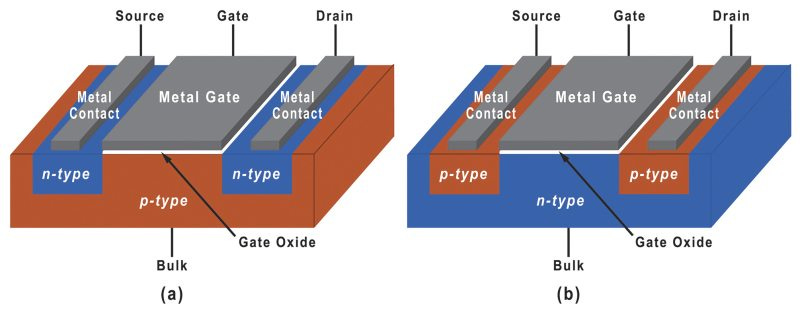
p and n-type semiconductors in a MOSFET, via MKS.
Early on, the primary method of introducing impurities in semiconductor manufacturing was diffusion: by heating the wafer up in the presence of a gas, atoms of the gas would diffuse into the wafer surface. But today doping is primarily done via ion implantation: a beam of ions (atoms with an excess or deficit of electrons, giving them an electrical charge) is fired at the wafer, depositing the atoms below the surface.
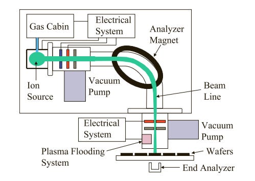
Ion implantation device, via Xiao 2012.
Heating
The last primary operation in semiconductor manufacturing is heating. There are many steps in the process where the wafer is heated or cooled to obtain a specific result. Ion implantation, for instance, results in a damaged silicon crystal structure. This damage is repaired with rapid thermal annealing; thermal lamps heat the wafer to over 1,000 degrees in a matter of seconds, and then the wafer is slowly cooled, repairing the crystal structure. Heating is also used during the lithography process to “bake” and harden the liquid photoresist.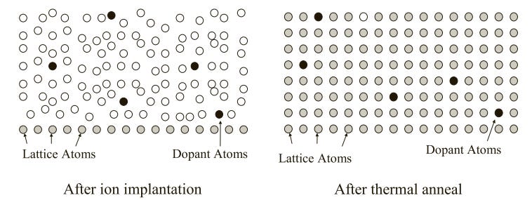
Via Xiao 2012.
In addition to these four basic processes, semiconductor manufacturing involves many other supporting processes. One key supporting process is polishing: because a microchip is built up from dozens of individual layers, variations in layer thickness will propagate over time as more layers are added, causing problems if left unaddressed. To combat this, wafers are frequently polished during the fabrication process using chemical mechanical polishing (CMP) to smooth out the wafer surface. CMP is also used to fill holes created by etching, by applying a layer of material to the entire wafer and then polishing away the material above the hole.

Wafer surface with and without CMP, via Chris Mack.
CMP used in the process of filling a trench with silicon dioxide, via Wikipedia.
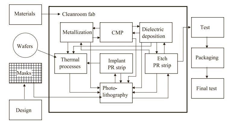
Another key supporting process is cleaning. Because the tiniest stray particle can cause a microchip to malfunction, wafers must be constantly cleaned with solvents and extremely pure water. In a modern fab, a wafer might get cleaned 200 times or more during the production process. And to ensure that processes are working correctly, fabs make extensive use of metrology — measuring the wafer at various points in the process to determine if there have been any manufacturing mistakes or defects.
Process flow diagram of a semiconductor fab, via Xiao 2012.
By applying these four basic processes over and over again, along with the various support processes, the structure of a microchip is slowly built up. And as more transistors have been crammed onto an integrated circuit, this structure (and the process for creating it) has become increasingly complex. Early integrated circuits could be made with just five to ten different masks and dozens of process steps, but a modern leading-edge microchip might require 80 or more masks and thousands of separate process steps.
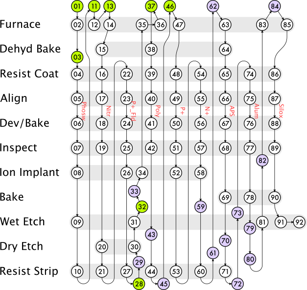
Process flow for a simple nine mask CMOS chip circa the 1980s, via Embedded Related. Today, leading-edge chips require 80 or so masks, and have much more complex process flows.
Once the wafer has gone through all these steps and the structure of the circuit is complete, it proceeds to assembly and packaging. This is where the wafers are cut apart into individual chips, each chip is connected to wires (and to any other chips, as with advanced packaging) and is encased in a protective coating. Packaging might be done at the semiconductor fab, or at another facility entirely.
Continued......
How to Build a $20 Billion Semiconductor Fab
For the last several decades, one avenue of technological progress has towered over nearly everything else: semiconductors. Semiconductors are materials that can have their conductivity varied by many orders of magnitude, which makes it possible to selectively block and allow the flow of...
 www.construction-physics.com
How to Build a $20 Billion Semiconductor Fab
For the last several decades, one avenue of technological progress has towered over nearly everything else: semiconductors. Semiconductors are materials that can have their conductivity varied by many orders of magnitude, which makes it possible to selectively block and allow the flow of...
www.construction-physics.com