DAC2025 SemiWiki 800x100

Wally’s u2u keynote

Wally’s u2u keynote
by Paul McLellan on 04-27-2011 at 3:25 pm

I was at Wally’s u2u (Mentor user group) keynote yesterday. The other keynote was by Ivo Bolsens of Xilinx and is here. He started off by looking at how the semiconductor industry has recovered and silicon area shipments are now back on trend after a pronounced drop in 2009 and revenue has followed. Finally the semiconductor business broke through the $300B barrier that it has nudged up against a couple of times in the past.

The Japan’s tsunami came along. With 22% of world semiconductor production Japan is the #1 area, slightly ahead of Taiwan (I was surprised by this, I assumed that Taiwan was #1, but Wally’s numbers are always rock solid). But things seem to be recovering reasonably fast and the current forecast is that world GDP growth will be 3.6% versus 3.9% before the tsunami, a real drop but not a catastrophe.

Over the last 20 years Japan has really specialized. Back then every company made VCRs, every company made TVs and so on. And there were (and still are) some odd combinations, Yamaha in musical instruments and motorbikes, for example. But now that Japanese companies have specialilzed, in many cases they have very large market shares of key ingredients to upstream processes. For example, one of the ingredients for black automotive paint was made in just one factory destroyed in the tsunami, leading to Ford being able to offer you a car in “any color you want as long as it is not black.” This combination of specialization and sole-sourcing has had tremendous economic benefit, not wasting learning by spreading it across multiple companies, reduced inventory and WIP. There risks being a backlash against this as a result of the disaster in Japan, moving towards dual sources and geographic dispersion. But there are huge increased costs associated with this, along with a decrease in R&D efficiency, reduce rate of quality improvement, increased inventories and so on.

EDA also has tremendous specialization. There are 68 product categories with more than $1M in revenue, almost all of them dominated by a single company: big segments dominated by big EDA companies and small ones by small companies. In many cases the #1 has over 70% market share and never less than 40% (for the big categories).

EDA has consistently been about 2% of semiconductor revenue, although that has gradually been declining since 2001 to 1.5%. Unfortunately, EDA headcount has been increasing faster than EDA revenue leading to huge pressure on costs and on the need for each company to grow its market share to get back in balance.

As Wally pointed out in his 2006 DAC keynote, EDA grows from new segments that spring into existence, become large and then remain at that size almost indefinitely. In 2006 he predicted lots of growth in DFM, ESL and AMS/RF and, lo, so it came to pass.

Looking forward, where will the growth come from? Wally’s predictions:

  • High level design: HLS, virtual platforms etc
  • Intelligent test-bench: automatic generation of tests scalable to multicore speedups, and integrated with emulation (including emulating the test harness too)
  • Physical verification and implementation. This is not a new area, of course, but the complexity of new design rules means that a completely new approach is needed to get a single pass flow that takes the real rules (including DFM, impact of metal fill on timing etc) into account early enough
  • Embedded software. The cost of designing the silicon of an SoC has been roughly constant for several years. But the cost of the embedded software for that SoC has exploded. There is an opportunity to take some of the re-use and automated verification from the silicon world into the software world.

The World’s Smallest Printed Circuit Boards: interposers

The World’s Smallest Printed Circuit Boards: interposers
by Paul McLellan on 04-27-2011 at 1:38 pm

Have you ever had the experience where you look up some unusual word in the dictionary since you don’t remember seeing it before. And then, in the next few weeks you keep coming across it. Twice in the last week I have been in presentations about the economics of putting die onto silicon interposers and the possibility of a new ecosystem growing up of bare microbumped die being available as a way of putting systems together. Sort of bringing multi-chip modules into the next generation.

The first was a presentation by Javier de la Cruz of eSilicon’s packaging department at the GSA 3D IC meeting. OK, so at a 3D IC meeting it is hardly news that someone was talking about silicon interposers. But he started from the basic economics that the increasing cost per tapeout drives down the number of tapeouts (there are other factors too, like the increasingly large volume needed to justify doing a state-of-the-art SoC). So there has to be another way to get custom hardware.

The other presentation was by Ivo Bolsens, the CTO of Xilinx. Obviously one of the ways to get custom hardware is to use an FPGA but in fact that was not what Ivo was talking about. He was talking about what he calls “crossover” ICs that combine features of ASICs, ASSPs and FPGAs. One way to do that is to create a tightly integrated processor subsystem combining processors, memories, some peripherals and FPGA fabric on one die. But the other way is to put separate die onto a silicon interposer.

Xilinx has been a leader in silicon interposer, using the approach to create large designs in new process nodes and get high yield. Xilinx calls this “more than Moore” approach “stacked silicon interconnect technology.” For the Virtex-7, instead of building a huge 28nm FPGA in a single die that would yield unacceptably, they put quarter array 28nm slices onto a 65nm silicon interposer (with tens of thousands of connections between the slices, this is not your father’s multi-chip Oldsmobile). See photomicrograph of a cross section to the left.

Interestingly, eSilicon had taken their yield models and analyzed a Virtex-7-like design and confirmed that by their numbers (they had no access to any internal Xilinx data) they were making a big saving. eSilicon estimated that in a 40nm process 24mm by 24mm baseline die compared to partitioning into four 24mm by 6mm die that the yield would go from 25% to 70%. Even with the additional cost of the interposer the cost saving looks to be over 50%. Pretty compelling. And Xilinx is actually at 28nm where the immaturity of the process should yield still more dramatic yield increase.

eSilicon has an approach that they call MoZAIC to allow them to put designs like this onto interposers to reduce the cost. There are three economic drivers that make this cost-effective: with pad limited die the interposer can fan out the I/O in a cheaper process, instead of building a large die in a very expensive process. Wth regular structures the partitioning can increase yield, as in the Xilinx case. And thirdly, it is possible to mix multiple technologies such as RF, FPGA, analog etc on a single interposer.

In the designs eSilicon had considered, some had negligible cost-savings and, in some cases, costs would increase. But some were very compelling. For example, one design contained 110Mb of 6-transistor SRAM plus more off-chip memory. By using an interposer, they could reduce the pincount (no external memory), remove the SRAM from the SoC, integrate the external memory onto the interposer and get a cost saving of 15% even without counting any saving due to no longer needing external memory on the board.

But the real attraction of this approach, that both Xilinx and eSilicon talked about, is if an ecosystem comes into existence where standard tiles are available to go along with custom tiles.

Two sweet spot customers for this approach could be mobile and networking. Mobile wants the lowest power and the smallest physical package, so integrating separate packages (e.g. radios etc) onto a single interposer has big potential gains. I know from a talk at the last DAC that Qualcomm for one is looking at this sort of approach. For networking, there are big limits on I/O count and huge difficulty (technical, power, testing) in using those limited pins to multiplex access to memory using DDR4/5. But with an interposer, very wide memory access is possible so complex memory controllers are not required.

Xilinx also see this as a attractive way to put CPU, memory and programmable logic into the same package, and with a lot more flexibility than the alternative where everything is integrated onto a single die with a single compromise on the amount of memory, programmable logic, number of cores and so on. I know from VLSI days years ago that putting memory onto a gate-array was really difficult because there was either too much memory or too many gates. If you did a custom base then you lost a lot of the advantages of gate-array that they could be turned quickly by pulling uncommitted arrays from wafer bank and adding the metal. It is easier to waste silicon now (and FPGAs are, by definition, wasting silicon for flexibility) but the same problem of finding the sweet spot exists.

eSilicon has started a prototype design to tape out this year to pipeclean the methodology. They have selected the partners for tiles (memory, IPD, FPGA, microprocessor, PHY), the tools, the IP, assembly and test partners. Xilinx are obviously ahead in this game, at least for the Virtex-7. It is worth noting that there is a lot of novel stuff in putting a design like this together. The interposer has through-silicon-vias (TSVs) and so has to be very thin, making it too fragile to handle as a wafer without attaching it to another piece of silicon or glass, which has to eventually be removed. There are many additional test issues since the tiles need to be tested (and tested well since a tile that slips through test onto the interposer results in discarding a lot of good tiles too). Then the final assembled system needs to be tested which requires careful thought about test architecture so that all the tiles can be accessed from external pins even if they are actually only connected internally to other tiles.


Semiconductor RTL Power Analysis: the sweet spot

Semiconductor RTL Power Analysis: the sweet spot
by Paul McLellan on 04-26-2011 at 4:20 pm

Power has become the strongest driver of semiconductor design today, more important than area, more important than timing. Whether the device is handheld, like a wireless phone, or tethered, like a router, complex power and energy requirements must be met. Shrinking geometries continue to impose new challenges as power management techniques and methodologies evolve to keep up.

Power consumption used to be verified at the gate-level, often too late to make any significant changes without major impact on the chip schedule. This is no longer good enough. The battery life of a handheld device can impact its competitiveness and the cooling and packaging choices for networking devices can make the profitability plummet. Power needs to be addressed and understood early in the design flow to have a meaningful impact.

Power management is not limited to lowering power alone. The design of the power delivery network (PDN) is a critical aspect of ensuring power integrity of the SoC. Excessive voltage sagging, for example, can cause timing failures or even result in the wrong value being latched. However, the impracticality of running gate level simulations means it is too late by the time vectors are available to identify some of these failure conditions (see figure which shows how a large change in current drawn by the chip coupled with package inductance can cause a large swing in voltage, and in turn in a timing failure ).

Instead, register transfer level (RTL) power analysis can be used to address power early in the design flow. At that level there is good visibility of where, when and why activity and power is going. It is the highest level of hardware abstraction where it has the capacity and performance to do full-chip power analysis while maintaining good accuracy. Moreover, RTL power can drive floorplanning and PDN design early in the design flow, versus traditional guesstimates and spreadsheets. During PDN power integrity sign-off, utilizing RTL simulations to uncover worst-case switching scenarios can also lower risks of potential chip failures.

Apache’s Power Model Methodology has three components, to manage power early in the design flow:

  • ·PowerArtist, which enables RTL power analysis and reduction. With simulation vector analysis, what-if exploration of different power architectures, automatic RTL power reduction, and a powerful environment for visual and textual power debug, it addresses power at RTL in all respects. In particular, RTL power metrics and analyses can drive key decisions on power grid and package.
  • ·RedHawk, which allows early PDN prototyping without compromising accuracy. With huge capacity, RedHawk is designed tohandle entire chips maintaining signoff accuracy and accurately calculates the effects of simultaneous switching nose (in core, memory and I/O), decoupling capacitance (intentional and intrinsic) and on-chip and package inductance. In particular, the power grid prototyping enables the on-die power grid required to meet the design’s power constraints coming in from PowerArtist.
  • ·The Chip Power Model (CPM) is Apache’s compact but Spice-accurate model of the full-chip power delivery network. Redhawk can create this to enable package selection and design with Sentinel, Apache’s chip-package-system (CPS) co-design, co-analysis solution.

During early stages of the design flow, when the major architectural and packaging decisions are still not finalized, the Apache methodology enables

  • ·Early PDN prototyping to facilitate optimum power grid sizing, supply pad and decap requirements, IO pad placement and floorplanning
  • ·RTL-power driven creation of a full-chip spice-accurate PDN model that can then drive early package design and selection

During sign-off, the Apache methodology enables:

  • ·Confidence signing off power integrity and package, via higher coverage across power-critical switching scenarios identified from RTL simulations
  • ·Superior realistic vectorless for power integrity analysis, guided by quantified RTL power data

In summary, full RTL to Silicon Power Integrity.

References:
Apache’s Power Model Methodology white-paper


How Avnera uses Hardware Configuration Management with Virtuoso IC Tools

How Avnera uses Hardware Configuration Management with Virtuoso IC Tools
by Daniel Payne on 04-21-2011 at 12:12 pm

Introduction
Here in the Silicon Forest (Oregon) we have a venture-backed, fabless analog semi company called Avnera that has designed over 10 Analog System on Chips (ASoC). Their chips are used in consumer products for both wireless audio and video applications.


James Rollins is the director of physical design at Avnera and I learned how they design these ASoC with Virtuoso and Hardware Configuration Management (HCM).

Questions and Answers

Q: What kind of IC experience does your design team have?
A: On average our team has over 18 years experience in areas like RF, analog, digital, DSP and embedded systems.

Q: Where do you design the chips?
A: Both here in Beaverton, Oregon and in California.

Q: What IC design tools do you have?
A: We use Cadence Virtuoso for our design environment.

Q: When you design blocks in your chips how many iterations would they typically go through?
A: Up to 50 iterations to get the desired low power, high audio quality and best wireless connectivity.

Q: Which HCM tool did you select?
A: ClioSoft has a tool called SOS that we use as our HCM.

Q: What were you looking for in a HCM tool?
A: Basically an HCM system that felt invisible to users, helped us automate our tool flow, enforced design conventions, and gave us notification of changes and a way to see changes.

Q: What was the install and setup like with SOS?
A: Within the first day we had SOS up and running the way we wanted it.

Q: How does SOS benefit your IC design process?
A: It protects our designers from accidentally loosing valuable data, plus it gets rid of manual tracking of design version details.

Q: Describe how your verification engineers use the HCM tool.
A: The DV engineers can configure different versions of the design as they perform verification. They can update test benches whenever parts of the design have been changed because they receive notification. For every test they know that the blocks are up to date.

Q: Does an HCM help you experiment a bit?
A: Our designers feel a little more free to play around to achieve the best results. You can experiment with subtle changes when you have a tool like SOS at your disposal. If a problem pops up, we can always roll back the changes.

Q: How did you get started with your HCM setup?
A: We had a meeting with ClioSoft to discuss our two design locations then decided to setup the SOS design data repository, a central filer in Oregon. In California we used a cache server that is automatically synchronized by SOS.

Q: Using that setup what is the benefit?
A: This has a major positive impact on network bandwidth requirements since a change in one block doesn’t not require copying the entire design or library during synchronization. A designer can go to any Avnera center and have access to their latest work.

Q: What does each designer see on their computer?
A: SOS gives each designer a private work area for their own development that can synch with all of the other work that is happening at the same time. A change made in Oregon can be seen by other designers in both Oregon and California.

Q: Would I use an HCM even with only one design center?
A: Yes, I’d use SOS even with a single design center. If you do have a remote office, then it’s mandatory.

Q: How does check-in work?
A: When the designer is happy with their work, they check-in that version so that it becomes available to the entire team. The design, documentation and the test bench for that block are all being managed by the SOS tool.

Q: When does a designer’s work area get updated?
A: The SOS tool can automatically handle that synch, but for our work we allow each designer control over when the synch happens.

Q: What kind of tool flow automation did you use?
A: With the ClioSoft tool we used the “Exec Before” and “Exec After” features during check in to run a set of automated tasks: netlisting of schematics, signal name compliance, and a “diff file” to show layout engineers what changed.

Q: Tell me more about visual differences.
A: We started using the Visual Design Diff (VDD) feature to automatically highlight the changes between two versions of a schematic or a layout. Inside of a Virtuoso editor window we can see the changes highlighted.

Q: When you integrate all of these analog and digital blocks into the final chip, what are the challenges?
A: It’s a challenge to debug the effects of top-level parasitics during chip integration. Small changes to a block’s behavior can make a large difference on the top-level routing and the parasitic values.

Q: How does the SOS tool help you with timing closure?
A: We do floor planning and routing, then run DRC and extraction to get a new netlist with parasitics. If timing or other measurements don’t meet spec then we can quickly switch out versions of blocks and then resimulate in order to pinpoint where the root cause is located.

Q: What other tips do you have for HCM users?
A: Use notes and tags to track your changes.

Q: Are you using compute farms in your design flow?
A: Yes, in Oregon we have compute farms and that lets our California designers remotely launch large jobs because the data is up to date and available.

Conclusion
Avnera is using Cadence Virtuoso IC tools with ClioSoft SOS as their HCM to successfully design ASoC chips for the highly competitive consumer wireless audio and video markets.

Also Read

Hardware Configuration Management and why it’s different than Software Configuration Management

Webinar: Beyond the Basics of IP-based Digital Design Management

Agile SoC Design: How to Achieve a Practical Workflow


Transistor-Level Electrical Rule Checking

Transistor-Level Electrical Rule Checking
by Daniel Payne on 04-20-2011 at 11:19 am

Introduction
Circuit designers work at the transistor level and strive to get the ultimate in performance, layout density or low power by creating crafty circuit topologies in both schematics and layout. Along with this quest comes the daunting task of verifying that all of your rules and best practices about reliability have been followed properly. While at Intel I debugged a DRAM design that had a yield loss issue caused by an electromigration failure, and this was at 6um design rules. We didn’t have any automated tools at that time to pinpoint where current density rules were exceeded. It simply meant that we created silicon, tested it, found reliability issues, fixed the issues, and re-spun another batch of silicon. This cost us valuable time to market delays.Lets take a quick look at several classes of circuits that would benefit from an Electrical Rule Checker (ERC) tool.

ESD Protection
Consider what happens at the inputs and outputs for each pad in your IC design for ESD (Electro Static Discharge) protection.

On the left we have an input pad with clamp cell, and in the middle an output pad with diode protection for overshoot and undershoot. For the input pad layout there are special rules for the current densities allowed in creating the series resistor as shown in the following diagram:

An ERC tool would need to read both the schematic and layout topologies, find the path from input pad to clamp cell, calculate current density along that path, compare current density versus the technology-specific constraints, and finally report any violations.A domain expert in ESD best practices should be able to program an ERC tool in order to automate the verification process.

Calibre PERC
Matthew Hogan is the TME at Mentor for their tool called Calibre PERC (Programmable Electrical Rule Checker) and he gave me an overview and demo last month. This tool automates the verification of transistor-level best practices in order to ensure first silicon success.

Multi-Power Domains
Portable consumer electronics like Smart Phones and Tablets are driving a large part of the semiconductor economy these days so it is import to have long battery life. This challenge is met by using a multi-power domain methodology where high speed sections have a higher power supply value than lower speed sections. Where these two power domains meet you need to insert a level shifter. PERC can verify if level shifters are in place.


Bulk Pin Connection
If your low-voltage PMOS device has the bulk connected to the wrong VCC supply it will function but also cause a reliability issue. With PERC you can write a rule to check for this condition:


Layout Based Verification
Rules can be described to find and report many classes important to reliability: Point to point resistance, current density, matching devices on a net, coupling de-cap placement, and hot gate identification.

Visualization
During the demo I saw the syntax for PERC rules and what happened when these rules were run on a test schematic and layout.

Each violation of a rule is highlighted, when I click a violation then I see both the schematic and layout windows appear and the violation is shown in red.

PDK
I think that the foundries will love this tool and should put in some effort to create and support PERC rules as part of their PDK (Process Design Kits). It’s really in their best interest to ensure first silicon success.

Conclusion
The Calibre PERC tool from Mentor combines ERC for both schematic and layout topologies so that you can enforce your own best practices across an IC design. Circuit designers can now use this methodology to check their designs for many classes (ESD, multi-power domain, AMS, etc.) of their circuits.


Thanks for the memory

Thanks for the memory
by Paul McLellan on 04-20-2011 at 1:26 am

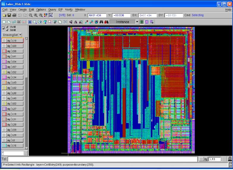
One of the most demanding areas of layout design has always been memories. Whereas digital design often uses somewhat simplified design rules, memories have to be designed pushing every rule to the limit. Obviously even a tiny improvement in the size of a bit cell multiplies up into significant area savings when there are billions of memory cells on a chip. It’s like that 9/10c per gallon at the gas station. It’s just a dime or so to you, but for Exxon it is real money.

Starting from its home base in Taiwan, Laker has been successful at capturing many of the big names in memory design in Asia. Hynix (based in Korea of course), Winbond and Eon (a newly public fabless memory company based in Taiwan) are all customers. Between them they cover DRAM, NAND flash, NOR flash and lots of specialized memory products for graphics and mobile.

But once you get outside the core itself, memory is no longer designed completely by hand, the automation from custom digital routing (driven off the desired connectivity) is an important part of productivity. To be useful in this sort of demanding layout environment it needs to be both gridded and shape-based, tuned for memory-specific routing styles such as main and secondary spine routing and limited routing layers (remember, memories like to keep metal cheap).

So memory layout is one of the most demanding application spaces of all. When I was at VLSI Technology our corporate counsel came from Micron and was amazed at the difference: “we put a design into production about once a year, here you do it about once a day.” Well, the memory market is no longer like that. It may not have quite the churn of new designs that a full-blown ASIC business does, but it is moving in that direction.

More information about Laker’s custom digital router here


Intel Buys an ARMy. Maybe

Intel Buys an ARMy. Maybe
by Paul McLellan on 04-19-2011 at 5:18 pm

Is Intel in trouble? Since it is the #1 semiconductor company and, shipping 22nm in Q4 this year with 14nm in 2013, it is two process generations ahead of everyone else it is hard to see why it would be. Intel, of course, continues to dominate the market for chips for notebooks, desktops and servers. But therein lies the problem. Pads are killing netbooks and nibbling at notebooks. These are not growing markets and actually are starting to gradually shrink. Instat reckons that in Q1 2011 PC volumes are down 2-3% from Q1 2010, largely due to incursion of iPads.

The growing markets are largely ARM-based: smartphones and iPad type computers. Intel’s approach to these markets has not been a success. First, after its acquisition of (part of) Digital’s semiconductor business it got StrongARM, renamed it Xscale, and invested something like a billion dollars in trying to penetrate the communications business. Eventually it disposed of that business to Marvell in a fire sale. Depending on what residual rights they retained this could turn out to have been an enormous strategic error. They didn’t just give up a ARM manufacturing license, they gave up a do-pretty-much-anything ARM architectural license.

Next up was Atom, a bet that whatever the sub-PC market was going to turn out to be that binary compatibility with Windows and with Microsoft Office would be a key differentiator. Intel even announced a sort-of deal with TSMC to allow people to build Atom-based SoCs but that didn’t seem to go anywhere and seems to have quietly faded away. Of course, iPad came along, closely followed by Android-based competitors. It seems clear now that Windows binary compatibility for this market is not something significant and, as a result, the entire Atom strategy has failed. At CES, the final nail was Microsoft announcing that even they didn’t believe x86 binary compatibility was that important and they would port some version of Windows to ARM (and, of course, WP7 already runs on ARM).

But Intel has a big fab to fill and it wants to grow. It has to compete with TSMC in process and leaders who use the ARM architecture in product. It is pretty clear that the only markets growing fast enough are ARM-based so Intel needs to have an ARM-based business. It doesn’t have time (and its track record doesn’t inspire confidence) to build one itself, so it will have to buy one. They could buy ARM themselves, perhaps, although that doesn’t directly help them fill their fab and has all sorts of antitrust issues I’m sure. Who else? The obvious candidate is TI’s OMAP business. TI are rumored to be shopping their wireless business around in order to focus on analog and DSP, maybe more so after the acquisition of National. The other big wireless businesses are part of Samsung and part of ST (well, actually the ST-Ericsson-NXP JV) but neither are likely to be for sale. And, of course, Qualcomm, but their market cap is already 2/3 of Intel’s and so that won’t fly. On the other hand, Qualcomm would have a hard time competing against an Intel ARM product line with two process generations’ lead.

The only other area of potential interest could be to pick up an FPGA business. It would pretty much have to be Xilinx or Altera to be big enough to help fill the fab. Of course these two approaches aren’t mutually exclusive, a big ARM business and an FPGA business should fill the remaining space in the fab.

TI/OMAP and Altera. Pure speculation, of course. We’ll have to wait and see.


Semiconductor Virtual Platform Models

Semiconductor Virtual Platform Models
by Paul McLellan on 04-19-2011 at 3:38 pm

Virtual platforms have been an area that has some powerful value propositions for both architectural analysis and for software development. But the fundamental weakness has been the modeling problem. People want fast and accurate models but this turns out to be a choice.

The first issue is that there is an unavoidable tradeoff between performance and accuracy; you have to give up one to get the other. But models that are fast enough for software development need to be millions of times faster than RTL and there is simply no way to get that sort of speedup automatically. Just as you cannot get from a Spice model to an RTL model by simply removing unnecessary detail, you can’t get from an RTL model to a virtual platform behavioral model by removing unnecessary detail.

Trying to create a model with both speed and accuracy seems to be the worst of both worlds. The model either has insufficient accuracy to be used for verifying the interaction of low-level software with the chip (in order to get higher performance) or else, if it has that accuracy, it will be too slow for software developers.

A better approach is to accept this and create both a high-speed model, for software development, and a medium-speed cycle-accurate model for hardware and firmware debug.

The medium-speed model can be created from the RTL automatically. Carbon Model Studio takes RTL models, completely accurate by definition, and delivers speedups of 10-100x by throwing away detail to produce a Carbonized cycle-accurate model. This guarantees the fidelity of the medium speed model to the actual chip.

Fast peripheral models, and in this context “peripheral” just means anything other than the processors themselves, are actually pretty simply to create in most circumstances. Often the peripherals have very simple behavior and the complexity in implementation comes from making them run fast in hardware: there’s close similarity between a 1 megabit Ethernet and a 1 gigabit Ethernet (or even 1 terabit) from a model point of view, for the implementation challenge not so much.

Of the solutions out there right now, this combination of a hand-crafted high-performance model (probably in SystemC) and an automatically generated medium-performance model that is guaranteed to match the RTL seems to be the closest that it is possible to get to the sweet spot. Like the old engineering joke about cheap-fast-good, pick any two. For virtual platform models it is fast-accurate pick one.


Semiconductor Industry Security Threat!

Semiconductor Industry Security Threat!
by Daniel Nenni on 04-17-2011 at 1:12 pm

The IBM X-ForceTrend and Risk Report reveals how 2010 was a pivotal year for internet security as networks faced increasingly sophisticated attacks from malicious sources around the world. The X-Force reportedly monitors 13 billion real-time security events every day (150,000 events per second) and has seen an increase in targeted security threats against both government and civilian organizations.

“The numerous, high-profile targeted attacks in 2010 shed light on a crop of highly sophisticated cyber criminals who may be well-funded and operating with knowledge of security vulnerabilities that no one else has,” said Tom Cross, threat intelligence manager at IBM X-Force. “Staying ahead of these growing threats and designing software and services that are secure from the start has never been more critical.”

Last year Iranian nuclear facilities were targeted. It first emerged in September that Iran was battling a powerful computer worm known as Stuxnet, which has the ability to send centrifuges — used in nuclear fuel production — spinning out of control. Different variants of Stuxnet targeted five Iranian organizations, with the probable target widely suspected to be uranium enrichment infrastructure. Iran confirmed that Stuxnet was found on mobile devices belonging to employees.

“Enemies have attacked industrial infrastructure and undermined industrial production through cyber attacks. This was a hostile action against our country,” Gholam Reza Jalali, head of a military unit in charge of combating sabotage, “If it had not been confronted on time, much material damage and human loss could have been inflicted.”

In its 16[SUP]th[/SUP] annual Internet Security Report, antivirus vendor Symantecdetected more than 286 million malware threats last year, signaling a big jump in the volume of automated cyber threats. Symantec gathers data from 240,000 points on the web in more than 200 countries and it gets intelligence from more than 133 million systems that use its antivirus products.

“We’ve seen seismic shifts in things like the mobile landscape,” said Gerry Egan, director of Symantec Research Labs. “The attacks are more sophisticated. There’s still a lot of education that has to happen to reduce the behavior that cybercriminals exploit.”

Last week WordPress.com revealedthat someone gained low-level (root) access to several of its servers and that source code was accessible and “presumed copied”. WordPress.com currently serves 18 million publishers, including VIPs Ebay, TED, CBS, Yahoo! and is responsible for 10% of all websites in the world. WordPress.com itself sees about 300 million unique visits monthly.

“We presume our source code was exposed and copied,” Mullenweg stated on the company’s blog. “While much of our code is open source, there are sensitive bits of our and our partners’ code. Beyond that, however, it appears information disclosed was limited.” Famous last words 😉

So what does this have to do with the semiconductor industry, an industry that is bound by dozens of EDA software vendors, IP companies, and design activity around the world? EVRYTHING! Think about how many people touch, directly and indirectly, an SoC design before tape-out? Use LinkedIn for example: My connections link me to 8,723,184+ people. The security risk probability for the semiconductor design ecosystem is staggering!

So when I see “security concerns” as the reason why fabless semiconductor companies CHOOSE not to get their designs into the cloud I laugh out loud. My guess is that it will take a catastrophic loss and/or jail time to get the semiconductor executives to protect intellectual property, the true assets of a company. Oh yeah, their financial assets are already safe and sound in the cloud!

Reference: 2011 Semiconductor Forecast: Partly Cloudy!


2011: A Semiconductor Odyssey!

2011: A Semiconductor Odyssey!
by Daniel Nenni on 04-15-2011 at 10:08 pm

Stanley Kubrick’s 2001: A Space Odyssey showed us a world where machine vision allowed a computer to watch and interact with its human colleagues. Yet after 40 years of incredible progress in semiconductor design, the technology to make computer-based image and video analysis a reality is still not practical.

While working with semiconductor IP companies in Silicon Valley I met Parimics, a very promising start-up focused on making real-time image and video analysis a reality. The company has created a unique architecture to make machine vision orders of magnitude more powerful, reliable and easy to use and deploy.

The key to Parimics’ image and video analysis subsystems is a novel image analysis processor chipset and accompanying software to deploy the technology. Vision systems based on Parimics’ technology are capable of processing image and video data in real time — right when the image and video data is taken. This is a huge advantage compared to current systems that perform analysis offline, i.e. after images have been captured and stored. Applications for the technology include automotive guidance; security and surveillance; medical and biotechnology applications such as f-MRI machines and high-throughput drug screening processes; advanced robotics; and of course generalized machine vision applications. Since these solutions are both deterministic and real-time capable, they can be used in scenarios that demand high reliability.

Image analysis solutions available today don’t have the speed or accuracy needed for complex machine vision applications. Speeds of 20 frames per second (FPS) or less are the rule. The ability to track specific objects is often limited to 3-5 individual items per frame. Filtering out noise and objects that are not relevant to the video analysis is poorly done with today’s systems. Finally, typical probabilistic methods greatly reduce system accuracy and trustworthiness. In some applications, it just cannot be tolerated that results are probabilistic or unreliable, or non-real-time.

In stark contrast, Parimics’ unique and patented architecture supports speeds between 50 to 20,000 FPS, and its results are deterministic and reliable. Even in the cost-optimized version of the processor chipset, Parimics’ solutions can track 160 unique objects per VGA or HD frame. The computational horsepower of the chipset also allows it to filter out noise and objects that are not relevant to the application within a very small number of frames.

Parimics’ architecture is specifically designed for advanced image analysis, much the same way that graphics processors are designed to create graphical images. The video analytics processors take in any type of image at any speed and use a massively parallel architecture to analyze all the objects in the field of view. Parimics’ scalable approach to solving customer problems easily meets the very wide range of their performance and cost requirements.

The company’s technical advisory board includes Stan Mazor, key inventor of Intel’s first microprocessor; John Gustafson, a leading expert in parallel architectures; John Wharton, inventor of the pervasive Intel 8051 microcontroller, and Dr. Gerard Medioni from USC, internationally known for his work on image recognition software.

Parimics’ founders, CEO Royce Johnson, and CTO Axel Kloth, have a combined experience of more than 50 years in chip design and management of cost-effective operations. See their web site at www.parimics.com for more details.