BannerforSemiWiki 800x100 (2)

Going up…3D IC design tools

Going up…3D IC design tools
by Paul McLellan on 01-23-2012 at 6:41 pm

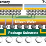
3D and 2.5D (silicon interposer) designs create new challenges for EDA. Not all of them are in the most obvious areas. Mentor has an interesting presentation on what is required for verification and testing of these types of designs. Obviously it is somewhat Mentor-centric but in laying out the challenges it is pretty much agnostic.

The four big challenges that are identified are:

  • physical verification for multi-chip packages using silicon interposers and (through-silicon-vias) TSVs.
  • layout-versus-schematic (LVS) checking of 3D stacks, including inter-die connectivity
  • parasitic extraction for silicon interposers and TSVs
  • manufacturing test of 3D stack from external pins

The first 3 challenges, updating the physical verification flow to handle 3D, are incremental improvements on existing technology. One complication is that the technologies (and hence the rules) used on each die may be different. But fundamentally, physical verification can be done one die at a time, LVS is comparing networks although bigger and more complex, and parasitic extraction can be done one die at a time although there are also inter-die effects that may need to be modeled. One area that does require a lot more attention is ensuring that the TSVs on one die do indeed match up to appropriate connection points on the die underneath so circuit extraction cannot be done entirely one die at a time.

The entire manufacturing process is obviously impacted by 3D in a major way. But here’s one less obvious area that is impacted: wafer sort. When a wafer comes out of the fab and before it is cut up into individual dice, it is tested to identify which die are good and which are bad. But at some point, enough testing is counterproductive: it is cheaper to waste money packaging up a few bad die and then discarding them at final test, than it is to have a much longer wafer test (perhaps even requiring more testers). When you discard a bad die at final test you are just wasting the cost of the package and the cost of assembly. The die itself was always bad.

With 3D this tradeoff point moves. If you package up a bad die along with several good die in a stack, then not only are you discarding a bad die, the package and the assembly cost. You are discarding all the other die in the package which are (most likely) good. So it makes sense to put a lot more effort into wafer sort. Plus, to make it worse, this is more likely to happen since, with several die in the package, the chance that all of them are good is lower than the chance that any one die is good.

Once the die are packaged up, then the challenge is to get test vectors to any die that are not directly connected to package pins. A very disciplined approach is required to ensure that vectors can be elevated up from the lowest die (typically connected to the package) and the upper levels.

Future challenges that are identified are:

  • architectural exploration. 3D offers another degree of freedom and all the usual floorplanning issues have to be extended to cover multiple-floors
  • thermal issues and signoff. TSVs and multiple die spread out heat to some extent, but nevertheless all the heat from the middle of the stack needs to get out
  • physical stress especially in areas around TSVs (where the manufacturing process can affect transistor threshold voltages)

The Mentor presentation is here.


High Speed USB 3.0 to reach Smartphone & Tablets in 2012… but which USB 3.0?

High Speed USB 3.0 to reach Smartphone & Tablets in 2012… but which USB 3.0?
by Eric Esteve on 01-23-2012 at 4:32 am

If you are not familiar with SuperSpeed USB standard (USB 3.0), you may understand this press release from Rahman Ismail, chief technology officer of the USB Implementers Forum, as simply claiming that USB 3.0 will be used in smartphone & media tablet this year… but, if you are familiar with the new standard, you are just confused! In fact, the nick name for USB 3.0 is “SuperSpeed”, as the nick name for USB 2.0 is “High Speed”. Calling USB 3.0 ‘High Speed USB 3.0” is just a good way to put confusion in the reader’ mind!

Let’s try to clarify the story.

  • High Speed USB (USB 2.0 running at 480 Mbit/s) is supported in Wireless handset for a while, allowing to exchange data with external devices (PC, laptop) and also to charge the battery (up to 500 mA). But, you also can find USB 2.0 used inside the handset for chip to chip communication only, it’s HSIC. Some chip makers use it for example to interface the Application Processor with the Modem, like TI in OMAP5.
  • SuperSpeed USB (USB 3.0 running at 5 Gbit/s) if offering a theoretical maximum data rate of 4 Gbit/s or 500 MB/s (due to 8b/10b encoding scheme of the PHY, similar to PCIe gen-2) and offers a battery charging efficiency almost twice better, up to 900 mA. Similarly, you can find SSIC, or USB 3.0 defined for chip to chip communication, used internally in the handset.
  • Adopting USB 3.0 will also bring additional benefits (SuperSpeed USB is a Sync-N-Go technology that minimizes user wait-time. No device polling and lower active and idle power requirements provides an Optimized Power Efficiency) but we will concentrate on data rate and battery charging here.
  • A very interesting opportunity has been offered when the MIPI Organization and USB IF have decided that MIPI M-PHY (specification for High Speed Serial physical layer, supporting data rates ranging from 1.25 Gbit/s to 5 Gbit/s) could be used to support USB 3.0 function. That is, a wireless chip maker can integrates USB 3.0 controller (digital) in the core and uses M-PHY instead of the USB 3.0 PHY. Because this chip maker is (or will) probably using MIPI M-PHY to support others MIPI specifications like UFS, DigRF or LLI, he will have already acquired the technology expertise and could avoid developing or acquiring a new complex PHY (USB 3.0), thus save time and money!

So far, the picture looks clear. Then comes the above mentioned press release from USB IF, saying:The data transfer rates will likely be 100 megabytes per second, or roughly 800 megabits per second (Mbps). Mobile devices currently use the older USB 2.0 technology, which is slower. However, the USB 3.0 transfer speed on mobile devices is much slower than the raw performance of the USB 3.0 technology on PCs, which can reach 5Gbps (gigabits per second). But transferring data using the current USB 3.0 technology at such high data rates requires more power, which does not fit the profile of mobile devices. “It’s not the failure of USB per se, it’s just that in tablets they are not looking to put the biggest, fastest things inside a tablet,” Ismail said.
To me, this PR from USB-IF represents another way to limit the attractiveness of SuperSpeed USB, able to offer 500 MB/s transfer rate, as this “High Speed USB 3.0” only offers 100 MB/s. Coming after the ever delayed launch of a PC chipset supporting native USB 3.0 from Intel, expected now in April this year when the USB 3.0 specification has been frozen in November 2008, it’s just like if a (malicious) wizard had decided to put a curse on SuperSpeed USB!

Will this standard has a chance to see the same adoption than the previous USB specification? Hum…

By Eric EsteveIPNEST– See also “USB 3.0 IP Survey


Analog Panel Discussion at DesignCon

Analog Panel Discussion at DesignCon
by Daniel Payne on 01-20-2012 at 7:59 pm

DesignCon is coming up and the panel discussions look very interesting this year. The one panel session that I recommend most is called, “Analog and Mixed-Signal Design and Verification” which is moderated by Brian Bailey, one of my former Mentor Graphics buddies and fellow Oregonian.
Continue reading “Analog Panel Discussion at DesignCon”


Acquiring Great Power

Acquiring Great Power
by Paul McLellan on 01-20-2012 at 5:11 pm

“Before we acquire great power we must acquire wisdom to use it well”
Ralph Waldo Emerson

Making good architectural decisions for controlling power consumption and ensuring power integrity requires a good analysis of the current requirements and how they vary. Low power designs, and today there really aren’t any other types, makes this worse since both clock-gating and power-gating can cause much bigger transitions (especially when re-starting a block) than in designs where the power is delivered in a more continuous way.

The biggest challenge is that good decisions must be made early at the architectural level, but the fully-detailed design data required to do this accurately is obviously not all available until the design has finished. But obviously the design cannot be finished until the power architecture has been finalized. So the key question is whether early power analysis can deliver sufficient accuracy to guide power grid prototyping and chip-package co-design and so break the cycle of this chicken-egg problem.

Early analysis at the RTL level seems to offer the best balance between capacity and accuracy. Higher levels than RTL don’t really offer realistic full-chip power budgeting and levels lower than RTL are too late in the design cycle and also are dependent on the power architecture. But even at the RTL level the analysis must take account of libraries, process, clock-gating, power domains and so on.

Getting a good estimate of overall power is one key parameter, but it is also necessary to discover the design’s worst current demands across all the operating modes. Doing this at the gate-level is ideal from an accuracy point of view but leaves it too late in the design cycle. Again, moving up to RTL is the solution. Clever pruning of the millions of vectors can locate the power-cricitcal subset of cycles consuming worst transient and peak power and dramatic reduce the amount of analysis that needs to be done.

Once all this is identified, it is possible to create an RTL Power Model that can be used for the architectural power decisions. In particular, planning the power delivery network (PDN) and doing true chip-package co-design. Doing this early avoids late iterations and the associated schedule slips, always incredibly costly in a consumer marketplace (where most SoCs are targeted today).

See Preeti Gupta’s full analysis here.


EDA Tool Flow at MoSys Plus Design Data Management

EDA Tool Flow at MoSys Plus Design Data Management
by Daniel Payne on 01-20-2012 at 4:50 pm

I’ve read about MoSys over the years and had the chance this week to interview Nani Subraminian, Engineering Manager about the types of EDA tools that they use and how design data management has been deployed to keep the design process organized. My background includes both DRAM and SRAM design, so I’ve been curious about how MoSys offers embedded DRAM as IP. They’ve basically made the DRAM look like an SRAM from an interface viewpoint (so no more RAS, CAS, OE complex timing).
Continue reading “EDA Tool Flow at MoSys Plus Design Data Management”


Intel Aims for the Upper, Upper Decks

Intel Aims for the Upper, Upper Decks
by Ed McKernan on 01-20-2012 at 3:07 pm

Since the introduction of Apple’s iPhone and then the follow on iPAD, it has been Wall Streets frame of reference that Intel would be playing defense as the PC market slid into oblivion and therefore a Terminal Value should be placed on the company. Intel’s Q4 2011 earnings conference call provided a nice jolt to the analysts as Paul Otellini signaled a massive Home Run to the Upper, Upper Decks is coming. The result of this is that a whole slew of Fabless Companies are about to get their functionality integrated into Intel’s smartphone, tablet and ultrabook platforms courtesy of the low power 22nm and 14nm trigate processes.

The old model was that Fabless was safe because it required little upfront capex outlay as the semiconductor market rotated in and out of boom and bust cycles. Therefore the higher P/E ratios accrued to Qualcomm, Broadcom, Altera, Marvell, Xilinx while Intel sat at a lowly 10 P/E. In addition, the Sovereign Debt Crises that had its beginnings over 10 years ago struck fear into ordinary investors who fled equity’s for the absolute safety of low yielding government bonds resulting in further P/E compression. However as Governments begin to print their way out of their massive liabilities, we may see a new safe haven for investors: the American export-oriented companies that sit on massive cash hordes and will be able to borrow at lower rates than the broke Sovereigns or their would be competitors.

Intel knows this and is leveraging its strong financial position into an even bigger investment in 2012 of 14nm capacity and R&D which can only mean that they are on a path to implement a mobile and datacenter roadmap that completely cannibalizes companies like Broadcom and Marvell in networking and the ARM camp in mobiles. The only possible holdout will be Qualcomm with their Communications IP.

On top of last years massive $10.8B Capex spending, Intel plans to spend $12.5B to build and outfit two 14nm fabs and thereby have in place by late 2013 twice the fab footprint they had in 2011 with 32nm. In addition, R&D spending is increasing 21% to $10.3B. That says there are a lot of tapeouts coming at 22nm and 14nm this year alone.

The revenue that Intel has guided to this year is only supposed to increase by “high single digits” so it means that they will only tag on an extra $5B to this years $54B. However, none of this takes into account the likely addition of Apple by end of the year and the fact that they are being very conservative on the uplift of ultrabooks vs today’s notebooks. A high ultrabook cannibalization or incremental growth scenario would mean much higher ASPs at the same volume as Intel charges a nice premium for low power.

Going into 2013, Intel plans to launch Haswell, which is a new microarchitecture that I would strongly speculate will take the TDP down from 17W for the ULV to under 10W. In the 1990s Intel’s business model paid more for higher MHz. Now the model pays for lower and lower TDP and higher integration. With a lower TDP, Intel will open up the next big revenue driver in tablets and ultrabooks, which is Intel 3G/4G/LTE baseband that will be common across all mobiles. Who wants to be limited by WiFi when Cellular is everywhere? Intel will argue that it’s communications solution in the latest trigate will overcome the power problems seen in the silicon coming out of the Fabless players and therefore ruin battery life and make enclosures more difficult to design.

Against this backdrop, it is important to remember that the other components in the tablet and ultrabook continue to drop in price (e.g. Screens, HDDs and Flash), which enables Intel to increase its relative BOM content in a rising unit volume market. Therefore tracking Intel’s revenue growth is more than linear with PC or Tablet unit growth.

If Intel succeeds with its plans, it will put tremendous pressure on TSMC and their ability to keep up as they rely on Qualcomm, nVidia, Altera and Broadcom to fund leading edge production. It also raises a question about Samsung’s plans to utilize Intel based solutions vs its internal ARM based chips. Samsung has been a long-standing PC player and will need to use Intel x86 in corporate tablets with Win 8. The smartphone and consumer tablet business is not just open for question, but open to Intel commoditization.

To accelerate the market move to Intel silicon in Smartphones and Tablets, Intel has just announced agreements with Motorola and Lenovo, the former home of Rory Read (CEO of AMD). Lenovo has been gaining share in the PC market at the expense of Dell and HP. With this deal, Intel is using the world’s lowest cost supplier to threaten the existing Android tablet and smartphone leaders HTC and Samsung. It will put extreme pressure on ARM processor suppliers later this year. The Motorola deal means that Intel will get preferential treatment in the tuning of the latest Google Android O/S for x86. ARM now will move to the back of the O/S bus.

The real story at the end of the day is that Moore’s Law is an even more destructive force than it was two years ago as the cost for the Fabless guys to play in Intel’s court has been raised dramatically. The Barbed Wire Fences Have Just Been Moved Out and Intel’s Ranch has grown.

FULL DISCLOSURE: I am Long AAPL, INTC, ALTR and QCOM


The Qualcomm PUT and The FABulous Year Ahead

The Qualcomm PUT and The FABulous Year Ahead
by Ed McKernan on 01-19-2012 at 5:14 pm

Humor can arise in surprising ways and yet still be disguised to many. As I was researching Qualcomm the other day, I came upon the transcript of their last quarterly earnings and I had to laugh. In the midst of last summer’s European crises, when the Club Med (Greece, Italy, Spain and Portugal) Sovereign Debt was trying to be rolled over with few takers and stocks swooned across the globe, there was Qualcomm injecting a little humor into the markets. You see, in the midst of everyone selling, did a very bullish thing: they sold over $500M of PUTS and collected $75M doing so. At the last earnings call, none of the analysts inquired. Why does a company with $21B in the bank sell PUTS to earn $75M? The answer, I believe has to do with Qualcomm looking to raise its profile even further as they separate themselves from the rest of the mobile ARM camp. However, 2012 will require an even bigger bet the company move.

Throughout the 1990s, Alan Greenspan, disciple of Ayn Rand, and perhaps the most knowledgeable person on the planet in terms of the gives and takes of the economy liked to befuddle congress with presentations that were incomprehensible with the result being that he had great degrees of freedom in pursuing a monetary policy that he believed generated optimum economic growth with low inflation and a stock market that for the most part headed north. An economy, though is a complex thing and even though he thought he could calibrate the health and dynamism by monitoring things like weekly cardboard box production, outside forces could take the stock market down (e.g. the Asian Crises in 1997 and LTCM in 1998). When a crises occurred he would swing into action by implementing what became known as “The Greenspan PUT”. The Fed would immediately lower interest rates and stocks would head higher to the cheers of the investment class. The PUT has limitations, as is seen in our current crises, when debt loads get too large.

Qualcomm’s PUT, in the midst of the European crises was a signal to Wall St. that they believe very good times lie ahead regardless of whether Italy, Greece, France or the whole EU goes in the tank. Although market indications lately show that Europeans will forsake everything to get their hands on an Apple iPAD and iPhone. Perhaps even Italian three hour lunches. Not to worry the money printing has already begun. So, Qualcomm’s selling of PUTS in Q3 was a bullish signal that at the time of expiration in 2H 2012, the stock will be higher than the strike price (I am guessing between $45 and $50 as Qualcomm’s stock flirted with a low of $46). Qualcomm said the breakeven price of the PUT option is roughly $43 a share. Below that they have to write a check to buy the stock back.

Qualcomm’s $21B stash of cash is greater than Intel’s and will soon be three times that of nVidia, Broadcom and Marvell combined who make up the ARM camp that not only are Qualcomm’s chief competitors but licensees. Qualcomm stands as a tall Redwood in a forest of seedlings as it is more than an order of magnitude larger in sales than any of the current ARM campers. But there are major business decisions coming down the pike.

Qualcomm, along with Intel and Apple have the most direct impact on the shaping of the smartphone, tablet, ultrabook mobile Tsunami marketplace and yet each impact it differently. Intel is driving ultrabook to be the form factor that separates them from nVidia and AMD giving them a de-facto Monopoly position in the PC space while also pursuing Apple for the iPhone and iPAD processor business. Apple, we know owns the iTunes Walled Garden Ecosystem that gives them the upper hand in selecting from a cornucopia of suppliers for its next products. You can say that Qualcomm is the winner no matter what communications solution is chosen – whether it is its own chipset or a royalty bearing solution from Broadcom, Intel, Marvell and others. However the big money is in supplying the chips and that can be a problem or opportunity.

As mentioned in previous blogs, the economics of Mobile Tsunami are different than the PC market. Apple and Samsung continue to go Vertical in their supply chain to remove excessive margins. In return for a capital investment and guaranteed demand, Apple gets vendors to drop ASPs and margins. Intel is approaching Apple with a production model that can retain its standard 50-60% Gross Margins but ASPs lower than Samsung due to their 2-3 year process lead. Qualcomm on the other hand sells chips that include the TSMC margin on top of their own 60%+ gross margin.

Bottom line: Does Qualcomm use its $21B cash to build a fab to eliminate TSMC margins and build next generation communications chips that aren’t available elsewhere? Do they approach Intel to Fab next generation standalone chips while offering Intel first rights on “volume integrated communications.” I don’t see Qualcomm moving to a complete IP model. However, the maturation of the very high volume mobile market combined with the economics suggest that the winners will either own Fabs or be IP Houses and a shakeout will take place among the Fabless. There is room for one profit margin, not two – unless you build at Intel. 2012 could be a very decisive year for Qualcomm.

FULL DISCLOSURE: I am Long AAPL, INTC, ALTR, QCOM.


What is a Hierarchical SPICE Circuit Simulator?

What is a Hierarchical SPICE Circuit Simulator?
by Daniel Payne on 01-19-2012 at 2:56 pm

Hierarchy is used in IC designs at many abstraction levels to help describe a design in a compact format:

  • Mask Data
  • IC Layout
  • Schematic Netlists
  • Gate level netlists
  • RTL netlists

But the question and focus for this blog is, “What is a hierarchical SPICE Circuit Simulator?”
Continue reading “What is a Hierarchical SPICE Circuit Simulator?”


NoC for faster SoC integration

NoC for faster SoC integration
by Eric Esteve on 01-19-2012 at 5:32 am

The need for Network-on-Chip (NoC) has appeared at the time where chip makers realized that they could really integrate a complete system on a single die to build a System-on-Chip (SoC). I was in charge of the development of a large IC, integrating different type of functions (Analog and Digital) to support advanced TV application. It was a long development, far to be easy, but the chip was not a SoC (even if at that time -1995- it was using the largest array available in TI ASIC technology). There was no integrated CPU, no SRAM and no High Speed Interconnect I/O. The SoC definition we agree in the industry is that the chip at least integrates a CPU (or GPU) core, then some amount of internal SRAM (or DRAM) and various peripheral functions specific to the Application. Considering this definition, “real” SoC designs have appeared in the early 2000. There are certainly exceptions to this rule, or designs integrating an embedded CPU earlier, but this were reserved to very high production volume projects.

When the chip makers have realized that Moore’ law was allowing complex SoC development, they understood that such development was only possible if they could assemble existing IP blocks (externally sourced or internally designed). Integrating various IP, each of these being a complete functional block, in a chip lead to the next problem to solve: how to efficiently interconnect these functions together and with the CPU (GPU)? Then came the need for something more efficient than just a crossbar switch (see previous post), a kind of “intelligent” interconnect system, say a Network, and because it’s to be internal, a Network on Chip: the NoC.

The above picture illustrate the move from the design of a Video Engine (in the 1990…), requiring a Village type of traffic when compared with a SoC design of the 2000 (OMAP4 from TI) requiring a City Traffic infrastructure. If we try to be more specific (and scientific!) we can say that a NoC is similar to a modern telecommunications network, using digital bit-packet switching over multiplexed links. Although packet-switching is sometimes claimed as necessity for a NoC, there are several NoC proposals utilizing circuit-switching techniques. This definition based on routers is usually interpreted so that a single shared bus, a single crossbar switch or a point-to-point network are not NoCs but practically all other topologies are.

Arteris’ FlexNoC interconnect IP product line generates a true NoC IP with distributed packetized transport and high-level SoC communication services, as opposed to a hybrid bus with centralized cross bars, as we have explained in this post.

Network-on-Chip (NoC) is an emerging paradigm for communications within large VLSI systems implemented on a single silicon chip. Sgroi et al. call “the layered-stack approach to the design of the on-chip intercore communications the Network-on-Chip (NOC) methodology.” In a NoC system, modules such as processor cores, memories and specialized IP blocks exchange data using a network as a “public transportation” sub-system for the information traffic. A NoC is constructed from multiple point-to-point data links interconnected by switches (a.k.a. routers), such that messages can be relayed from any source module to any destination module over several links, by making routing decisions at the switches. A NoC is similar to a modern telecommunications network, using digital bit-packet switching over multiplexed links. Although packet-switching is sometimes claimed as necessity for a NoC, there are several NoC proposals utilizing circuit-switching techniques. This definition based on routers is usually interpreted so that a single shared bus, a single crossbar switch or a point-to-point network are not NoCs but practically all other topologies are. This is somewhat confusing since all above mentioned are networks (they enable communication between two or more devices) but they are not considered as network-on-chips. Note that some articles erroneously use NoC as a synonym for mesh topology although NoC paradigm does not dictate the topology. Likewise, the regularity of topology is sometimes considered as a requirement which is, obviously, not the case in research concentrating on “application-specific NoC topology synthesis”. Let’s add that the first dedicated research symposium on Networks on Chip was held at Princeton University, in May 2007… pretty recent, isn’t it?

To learn a lot more about NoC and Arteris products, just go here.

By Eric Estevefrom IPNEST


Apple 4S nearly catches up to Android, perhaps

Apple 4S nearly catches up to Android, perhaps
by Paul McLellan on 01-19-2012 at 4:00 am

Apple’s iPhone did well in Q4 according to Neilsen who polled recent buyers of smartphones. Of people who had purchased a smartphone in the previous 3 months (roughly Q4) 44.5% chose an iPhone (up from 25.1% in October, roughly Q3). But Android retained the lead with a 46.9% share, down from 61.6% in October. How many phones are we talking about? Apple is expected to announce in its earnings call that it sold over 30M iPhones last quarter. Happy Holidays lots of people.

To be honest, I think these numbers are a lot less significant than they sound. The latest iPhone, the 4S, went on sale on October 14th. Everyone knew it was coming and so most people who wanted a new iPhone waited until then. So Q3 numbers for Apple were temporarily depressed and Q4 numbers were temporarily boosted. If we guess that half the difference is this one-off kick (and I have no idea if it is) then iPhone is really 35% and Android is really perhaps 60% leaving everyone else with crumbs (Blackberry, Nokia+WP7).

As long as Apple continues to post numbers in this sort of range, and doesn’t retreat to, say, 20% market share then it wins. It has enough of a base that people will want to write apps for it (you make more money on an iPhone app than an Android app) and Apple will take almost all the profit out of the smart phone hardware market (or even the whole cell-phone hardware market since the non-smart-phones (stupid-phones?) don’t make much profit especially at the low-end).

Android hardware manufacturers like HTC simply do not have the high margins that Apple has, they have the margins of a typical PC manufacturer of a few percent. It will be interesting to see if Motorola, soon to be part of Google, can get any sort of price premium or even if Google wants to go that route, as opposed to flooding the world with as many Android phones as it can. It is not clear to me that buying Motorola, pretty much giving away the phones, and making it back on search (versus trying to build it into a profitable business in its own right) would be a good idea. Yes, Google makes most of its money on search, but that’s no reason not to try to make money elsewhere.

There was some noise at CES about handsets, mostly around the (I believe very serious) entry of Intel into the cell-phone SoC market rather than the handsets themselves. But CES is not the big show for cell-phones, that would be the Mobile World Congress at the end of February in Barcelona (used to be called GSM Congress back when it used to be in Cannes). So it will be interesting to see if there are significant announcements there.