Bill Gross, founder and co-chief investment officer of PIMCO, the world’s largest Bond Fund, recently declared, “We’re Witnessing the Death of Equities.” Contrarians should take note as Gross made a similar calling 10 days before the previous major stock market bottom on March 9[SUP]th[/SUP] 2009. For Entrepreneurs and Venture Folks who are essentially “equity innovators”, I would like to suggest that these declarations of end times probably mark the start of a new up cycle similar to what occurred in the 1980s and 1990s. Prior to that there was a generational stock market bottoming that coincided with the Business Week magazine cover of August 13, 1979 Titled: “The Death of Equities.”
Continue reading “"Death of Equities" = A Silicon Valley Revival”
Traditional Model of Funding Semiconductor Equipment is Broken?
At Semicon a few weeks ago the big news was that Intel was making a big investment in ASML as a way of funding two development programs: extreme ultra-violet (EUV) and 450mm wafers. This week TSMC announced that they would join the program too, committing 275M Euros over a five year period. They are also taking a 5% stake in ASML. ASML have said that they are also talking to some other smaller vendors.
Both these investments are a sign that the traditional model of funding semiconductor equipment is broken. Historically, the equipment companies would fund the investment out of their revenues and recover it by selling equipment. Two things have changed though. The first is that the cost of the development has grown huge, too risky for the equipment companies to undertake on their own without a level of risk sharing with the semiconductor manufacturers. The other problem is that nobody knows how many more process generations there will be that use this new generation of equipment.
In effect, the equipment industry is no longer generating enough profits to fund the investment needed for the future and it is unclear whether there are enough process generations still ahead to recover the cost of that investment.
I’ve said before that there are a lot of risks in EUV. The one that gets all the attention is that the light sources are one to two orders of magnitude dimmer than they need to be. However, two problems with masks also seem severe: mask blanks are not defect free and any particle that gets on the mask is in the focal plane of the mask and so will print, unlike refractive masks that have a pellicle to keep particles away from the plane of the mask itself.
450mm is also a big risk. SEMATECH estimates that the 300mm transition cost between $25-30B and it is not clear if that is actually being recovered. The transition to 450mm is even more challenging. Every piece of equipment must be changed, a huge number of test wafers will need to be manufactured. If EUV works as advertised then we will have a single patterning technology so that each layer on the wafer only needs to be processed once. However, if EUV does not deliver then we will continue to need to use double, triple, quadruple patterning. There are some economies of scale with 450mm since the wafers only need to be changed in the stepper half as often, but a die exposure takes the same length of time whatever the size of the wafer and so each layer of the wafer benefits little from the increased wafer size during lithography.
But the biggest challenge with 450mm is just how many more process generations there will be before we need to go to something different that uses, presumably, different equipment. The earliest that EUV and 450mm wafers might arrive is to be retrofitted to 14nm. It is already too late for the first scheduled 14nm production. At Semicon an Intel fellow said that they are basically almost freezing the design rules for 9nm with the assumption that EUV will not be available and assuming multiple patterning will be required.
Conductive Bridging RAM ( CBRAM )
One area of the Semiconductor Market that has continued to see start-up venture investment is emerging memories. There is always a perception and need to discover a memory that can either displace the current technologies or create a new niche between DRAM and Flash. Adesto Technologies was founded in 2007 to explore and commercialize CBRAM (Conductive Bridging RAM) as a product and as an embedded IP. CBRAM is of a class of Resistive RAMs that are low voltage, non-volatile and built in standard CMOS processes. CBRAM can scale with CMOS technology and is fundamentally lower in power than Flash. I can see a number of applications here including embedded SOCs such as microcontrollers.
With its CBRAM™ technology, Adesto has now become a leading contender in providing a low cost, low power alternative to Flash memory for a wide range of embedded applications. In addition, given that CBRAM memory can scale with Moore’s Law in standard CMOS for many generations to come, Adesto has the potential of being a significant long term provider of high density, non-volatile memory solutions. Alan J. Niebel Web-Feet Research
Adesto is shipping its first product, an EEPROM replacement device that was built in a standard .13u process technology at a die size that is smaller than traditional solutions. In addition, it has licensed its technology to multiple semiconductor firms who plan to embed it with future devices. It’s an exciting market. Feel free to explore more at www.adestotech.com.
Because there is a lot of research and interest in the field of resistive RAMs, Adesto has initiated and sponsored the creation of a forum that focuses on these new developments. The site is run by an independent moderator, Mr. Christie Marrian. He would be glad to hear from readers and folks interested in contributing articles. The site can be found at www.ReRAM-Forum.com:
We are starting this Blog as a home for articles and discussion related to memory technology based primarily on resistive change (commonly known as RRAM or ReRAM) and conductive bridge (commonly referred to as CBRAM). We are open to anyone actively interested or working in the field. It is timely as RRAM/CBRAM are rapidly gaining traction both as viable technologies in their own right as well as solutions for the scaling limitations of conventional flash memory. We envisage that we will have both technology push and application pull entries and aim that the Blog will become the first ‘port of call’ for potential users as well as those following the latest developments in this exciting field.
Technology related:
- RRAM/CBRAM Technology Overviews
- New System Architectures
- Technology Updates
- News Items
Application related:
- Market Analysis and Forecasts
- Product Announcements and News
- Application ‘Pull’ describing applications where RRAM/CBRAM technologies are well suited
The RRAM/CBRAM Blog is a moderated Blog in order to ensure that it maintains focus. We also encourage comments which will also be moderated.
Christie Marrian, WWW.ReRAM-Forum.com Moderator
CEVA-MM3101 DSP IP core
If the CEVA-XC4000 DSP IP core offers support for the most demanding communication standards, the CEVA-MM3101 provides full control over embedded vision and image enhancement applications, in SW, allowing Application Processor chip makers and OEM a way to differentiate their product. CEVA has decided to launch the MM3101 to help Application processor chip makers to overcome several barriers. If the ARM + NEON solution is selected, it quickly appears to be a low performance option. Choosing a GPU is an option which implies high power consumption. Selecting a solution based on HW accelerators, or fixed functions, is suffering from a strong lack of flexibility for SW upgrades.
OEM, the first customers for the Application processor IC, looks to differentiate, on such a competitive market segment, smartphone and media tablet. Integrating MM3101 will allow designing in-house SoC and would enable applications not available on other devices. Thus, unique and innovative algorithms can be easily programmed on the device. The result, in term of power consumption, is impressive: running such apps on the MM3101 can save 10X or more, as opposed of running on the CPU or GPU.
CEVA-MM3101 solution can be illustrated by the various layer descriptions, as in the picture: at the bottom, the hardware platform (HW layer), then the Library Layer, the Interface Layer and finally the Application layer. CEVA can propose solution for Image Enhancement, Embedded Vision and Scene Analysis, either with products developed internally, either with products developed by partners like Khronos Group, completed by commercially available tools like Optimizing C compiler, Multi-core debugger and so on.
To take an example, illustrating the computing power of the MM3101, just have a look at Super Resolution. This is an amazing algorithm: by fusing several low resolution images to generate a (single) high resolution image that offers more details. As a good picture is always better than a long explanation, just take a look at the following images:
Using the MM3101 Super Resolution algorithm allows generating the High Resolution Image. Amazing!
This is just one example of one of the multiple solutions offered by the MM3101 DSP IP core from CEVA, targeting imaging enhancement for application processor, one of the hottest area in the smartphone and media tablet segment. Using such a core can help OEM and Application processor chip makers to differentiate, and differentiating will help them to consolidate or increase market share, in this very competitive market segment, where the projection call for more than 600 million devices to be shipped in 2012, and the 1 billion level to be passed by 2015!
BY Eric Esteve
TSMC Leads Semiconductor Sales Growth in 2012!
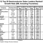
As a fitting postscript to my “Brief History of the Fabless Semiconductor Industry”, semiconductor research company IC Insights compiled a list of the top semiconductor companies for the first half of 2012. As the traditional IDMs go fabless and sink in the ratings, the foundries post record gains led by TSMC at 22%, GlobalFoundries at 18%, and UMC at 16%, WOW! GlobalFoundries also passed UMC for the #2 spot with $2B in Q1/Q2 2012 revenue versus $1.8B. You go GloFo! TSMC is still the foundry market segment leader with $7.9B.
In case you are not familiar with them, IC Insights is a leading semiconductor market research company offering coverage of current business, economic, and technology trends, top supplier rankings, capital spending and wafer capacity trends, the impact of new semiconductor products on the market, and other cool semiconductor industry information. I really like these guys, they are a bloggers best friend.
The biggest losers here are the Japanese IDMs; Toshiba, Fujitsu, and Renases which declined 26%, 23%, and 10% respectively. While Toshiba is riding the memory pricing rollercoaster, Fujitsu and Renases are in transition to the fabless business model moving manufacturing to TSMC. AMD also took an 11% hit which is not surprising as the company is still in “flux”. Check the blogs “The Coming Battle for AMD’s x86 Hidden Cache” and “AMD 2Q Financials — The Good, The Bad, and The (Pretty) Ugly” for more information on AMD.
U.S. Memory maker Micron moved up one spot with a 5% increase in sales. As Micron digests Japanese memory maker Elpida, expect another spot or two jump with an additional $2-3B in sales. Elpida is the last Japanese DRAM maker so this is an end of an era for the Japanese semiconductor industry. How long before Japan is completely fabless? Certainly within my lifetime (I’m 51).
Qualcomm, the fabless semiconductor wonder, posted a surprising 6% decline. Rather than taking personal responsibility, Qualcomm CEO, Dr. Paul E. Jacobs Ph.D, blames 28nm supply shortages even though Qualcomm is working with multiple foundries and I can tell you that TSMC has fulfilled ALL contractual commitments for 28nm. Either Qualcomm is bad at forecasting demand or this finger pointing is a diversion for deeper problems at Qualcomm. As TSMC clears all 28nm backlog in Q3 let’s see where the finger points at the next Qualcomm conference call. You can bet I will blog it because I really hate finger pointing. In stark contrast, the non-finger pointing Broadcom posted an 8% gain. And the mighty Intel posted a disappointing 5% increase based on lackluster Ultrabook sales and no position at all against ARM in the mobile market as of yet.
All-in-all a good financial start for what will be a great year in semiconductors. 28nm is breaking ramping and revenue records, 20nm tape-outs will commence in Q1 2013, the mobile market segment continues its meteoric rise, and the semiconductor ecosystem has never been stronger. So, do you still think that the fabless business model is broken Mr. Mark Bohr of Intel? I’m also not a fan of asinine PR stunts so I will continue to haunt Intel on this one.
Mars Rover "Curiosity" and EDA
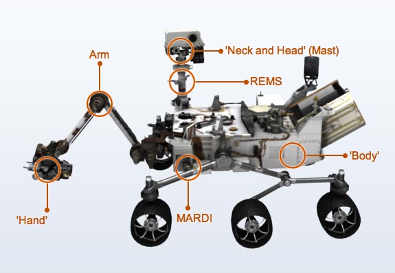
I’m watching the latest Mars rover landing tonight called “Curiosity” and wondering about all of the electronic systems designed to control the project and hopefully send back some stunning new images along with new data on the micro-biology and chemistry of the red planet. JPL gets all the glory for designing and building this mission, however without EDA tools used in the design of electronics none of this planetary exploration would be possible. Continue reading “Mars Rover "Curiosity" and EDA”
A Brief History of EDA
Electronic Design Automation, or more affectionately known as EDA, is a relatively young $5B industry with a very colorful upbringing, one that I have experienced firsthand, I’m very grateful for, and is an honor to write about. Today EDA employs an estimated 27,000 people! There is a nice EDA Wikipedia page which can be found here.
Before EDA, integrated circuits were designed by hand. Automation first came with geometric software to generate the tapes for the Gerber photoplotter, but even those copied digital recordings of mechanically-drawn components. The process was fundamentally graphic with the translation from electronics to graphics done manually. The best known company from this era was Calma whose GDSII (Graphic Data System) format is still an industry standard. In 1984 my first job at Data General was to support Calma, the Calma II station was based on Data General Eclipse hardware.
By the mid-70s, developers started to automate design with many tools including place and route (P&R). The proceedings of the Design Automation Conferences(DAC) cover much of this era. The first DAC I attended was 1984 in Albuquerque, New Mexico, which was the first DAC with vendor exhibits, and I have not missed one since. That DAC was VERY entertaining and not much different from my time at Chico State University! 😎
The next era began about the time of the publication of “Introduction to VLSI Systems” by Carver Mead and Lynn Conway in 1980. This ground breaking text advocated chip design with programming languages that compiled to silicon. The immediate result was a considerable increase in the complexity of the chips that could be designed, with improved access to design verification tools that used logic simulation.
1981 marks the beginning of EDA as an industry. For many years, the larger semiconductor companies (IDMs) developed EDA software internally. In 1981, executives and engineers spun out of these companies to concentrate on EDA as a business. Daisy Systems, Mentor Graphics, and Valid Logic Systems were all founded around this time, and collectively referred to as DMV. Within a few years there were many companies specializing in EDA, each with a slightly different emphasis.
EDA really came into its own with the advent of the ASIC business pioneered by companies like VLSI Technology and LSI Logic. Using excess Japanese manufacturing capacity and building their own fabs locally, they produced Application Specific Integrated Circuits (ASICs) and offered ASIC services for emerging fables semiconductor companies. A few years later TSMC introduced the fabless semiconductor business model promoting manufacturing efficiencies and commercially available EDA software.
In 1989 the EDA Consortium (EDAC) was founded “To promote the health of the EDA industry, and to increase awareness of the crucial role EDA plays in today’s global economy.”Currently EDAC represents approximately 100 companies around the world. There is a nice 15 minute promotional video “Where Electronics Begins” HERE.
Today Synopsys, Mentor, and Cadence are the dominant players. There is a very interesting EDA Mergers and Acquisitions Wiki which chronicles the evolution of EDA companies. This is one of the most active Wikis on SemiWiki!
Where would the semiconductor industry be without EDA? I hate to even imagine! The EDA industry makes it possible for the world’s electronic companies to satisfy demand for smaller, faster, more power efficient, and lower cost electronic products. A very clear example: EDA has enabled billions of mobile devices around the world! Believe it!
A Brief History of Semiconductors
A Brief History of ASICs
A Brief History of Programmable Devices
A Brief History of the Fabless Semiconductor Industry
A Brief History of TSMC
A Brief History of EDA
A Brief History of Semiconductor IP
A Brief History of SoCs
Synopsys Challenges with SpringSoft Acquisition
Another week in EDA and yet another acquisition by Synopsys as they buy SpringSoft this time for $406 million in cash. Paul McLellan wrote a good blog on this merger too.
Last week I blogged about the product overlap and integration challenges that Synopsys faces with the acquisition of Ciranova.
Let’s take a look at the IC entry and layout products from SpringSoft and how they fit into the tools that Synopsys already owns:
Continue reading “Synopsys Challenges with SpringSoft Acquisition”
Synopsys Aquires Springsoft
Today it was announced that Synopsys is acquiring SpringSoft for $406 million dollars ($12.2B Taiwanese). Coincidentally, I was in SpringSoft’s US office yesterday to talk about how Laker is being used for 20nm design. More of that later. But there was certainly nothing to indicate that anyone there was expecting this.
Last week Synopsys acquired Ciranova. They had some good technology for analog automation but it seems clear with this acquisition that Synopsys just wanted to ensure that the Ciranova PyCell technology remained viable and found a home. With the acquisition of Laker, Synopsys has a much stronger position in layout in general and analog automation in particular.
The other part of SpringSoft is the Verdi verification environment. In another odd coincidence, just a few days ago I wrote about the integration of the Synopsys Protocol Analyzer with SpringSoft’s Verdi through the open VIA interfaces that Verdi has provided for about a year now. I guess that integration like that might get a bit tighter going forward.
The verification market is split three ways with Mentor, Cadence and Synopsys all having strong positions. Verdi strengthens Synopsys’s position, of course, but it doesn’t really upset the balance of power enough to put them convincingly ahead. Plus, verification is one of the areas where customers seem to like to have more than one solution, both since the different solutions have different capabilities and to give a stronger negotiating position. Many customers use Verdi with Cadence and Mentor simulators so whether Verdi grows or shrinks as a business due to the acquisition is an open question.
The layout market is the one where this might make a big difference. Cadence has had a dominant franchise in this market with their Virtuoso environment. The lock-in has been the thousands of lines of SKILL code that customers have written and that nobody else can support. One thing I learned yesterday is that 20nm is so different that most of that SKILL is irrelevant and even PDKs are less important since there is so little flexibility about how transistors can be created. The 20nm changes along with the newish analog automation has created an opportunity for SpringSoft’s Laker. Laker has been very strong in Taiwan (SpringSoft is headquartered there) but has recently started to get traction in more and more big name companies outside of its home base. With the Synopsys name and sales channel this could really even up the layout playing field.
Or maybe not. One of the weird things about EDA is that the big sales channels cannot sell products that the customer isn’t asking for. So much of their revenue comes from reselling what they sold last time they don’t like to jeopardize the big deal with a product where they have to work to displace an incumbent. When Cadence acquired Ambit’s synthesis, the sales channel refused to sell it and continued with their strategy of “concede synthesis to Synopsys and try and get the rest of the budget.” Let’s see how good Synopsys’s sales force is at displacing Cadence’s Virtuoso of if they adopt a “concede layout to Cadence and try and get the rest of the budget.”
Since this doesn’t give Synopsys a dominant position in functional verification and since Cadence is the dominant layout incumbent, not Synopsys, I can’t see that this deal is likely to get major regulatory oversight. It is far less contentious than Synopsys acquiring Magma, giving them a second place and route solution, and Finesim, and Tekton static timing, areas where Synopsys was already the leader.
In yet another odd coincidence, the first I knew about the acquisition is that I got an email from Tony Trousset of Atlas Technology Ventures that they had acted as advisers to SpringSoft in the transaction. I’ve not heard from Tony for ages, but he was at Deutche Bank when he was one of our advisers when we sold Compass while I was CEO (eventually to Avant!) back in 1998.
Arteris FlexNoC penetration increase… everywhere
The need for Network-on-Chip (NoC) has appeared at the time where chip makers realized that they could really integrate a complete system on a single die to build a System-on-Chip (SoC). At the early times (1995-2005), the so-call NoC IP suppliers were in fact proposing a crossbar switch, a pretty old concept initially developed for Telecom applications where you had to switch between multiple users, every signal (user) having the same priority.
When the chip makers have realized that Moore’ law was allowing complex SoC development, they understood that such development was only possible if they could assemble existing IP blocks (externally sourced or internally designed). Integrating various IP, each of these being a complete functional block, in a chip lead to the next problem to solve: how to efficiently interconnect these functions together and with the CPU (GPU)? Then came the need for something more efficient than just a crossbar switch, a kind of “intelligent” interconnect system, say a Network, and because it’s to be internal, a Network on Chip: the NoC.
The above picture illustrate the move from the design of a Video Engine (in the 1990…), requiring a Village type of traffic when compared with a SoC design of the 2005 (OMAP4 from TI) requiring a City Traffic infrastructure. If we try to be more specific (and scientific!) we can say that a NoC is similar to a modern telecommunications network, using digital bit-packet switching over multiplexed links. Although packet-switching is sometimes claimed as necessity for a NoC, there are several NoC proposals utilizing circuit-switching techniques. This definition based on routers is usually interpreted so that a single shared bus, a single crossbar switch or a point-to-point network are not NoCs but practically all other topologies are. Arteris’ FlexNoC interconnect IP product line generates a true NoC IP with distributed packetized transport and high-level SoC communication services, as opposed to a hybrid bus with centralized cross bars.
Since 2005 and the start of Arteris, FlexNoC, their flagship product, has made his way, initially in the wireless segment (I may be wrong, but I think Texas Instruments was Arteris very first customer, the FlexNoC being integrated into OMAP, the Application Platform for wireless phones/smartphones), rapidly gaining market share in this very demanding, competitive segment. Most of the time, the real competition was with internally developed solution. Everybody who had to compete with the Non-Invented-Here (NIH) syndrome knows how difficult it can be: you may have the best product, the NIH make it very difficult to sale! When looking at Arteris web site, you can see that the company is selling now in Wireless, Video and Imaging, Networking, Automotive and Consumer segments. That you see is also the fact that these customers are mostly located in USA, Korea and Japan. Europe and the rest of Asia was a virgin territory for Arteris… until very recently, on July the 19[SUP]th[/SUP] to be specific, when a press release was announcing that Rockchip had acquired the FlexNoC IP from Arteris.
Which is very interesting is that the company is a “leading Chinese fabless semiconductor company and mobile internet System-on-Chip (SoC) provider will leverage the chip in new cost-effective Android-based tablets and other mobile devices”. The NoC penetration in China is a strong signal: it means that Chinese fabless are playing in the same space than the TI, Qualcomm or Samsung. It also means that the Network-on-Chip, just a concept ten years ago, is penetrating every segment, every region of the world. One reason can be found in Rockchip quote from Li Shiqin: “We evaluated all the leading interconnect technologies and proved that Arteris’ NoC technology is the good choice for our multicore ARM-based SoCs,” said Li Shiqin, IC Design Manager at Rockchip. “Arteris FlexNoC is the suitable way for us to meet our design frequency, power, memory efficiency and QoS requirements.” The combination of Rockchip’s high-performance, energy-efficient processor and Arteris’ FlexNoC interconnect IP will deliver a robust platform for data-intensive tablet applications. These key benefits will translate to faster time-to-market for Android table manufacturers striving to meet fast changing consumer demands.
We also should quote Charles Janac: “Rockchip’s reliance on Arteris FlexNoC as the SoC interconnect within their most important platforms speaks volumes for Arteris’ unique network-on-chip technology,” said K. Charles Janac, President and CEO of Arteris. “Arteris NoC technology resolves key system bottlenecks ? and delivers significant technological and economic benefits.”
To learn a lot more about NoC and Arteris products, just go here.
By Eric Estevefrom IPNEST


