An empty Fab is a terrible thing to waste, especially when it is leading edge. By the end of the year Intel will, by my back of the envelope calculation, be sitting with the equivalent of one idle 22nm Fab (cost $5B). What would you do if you were Paul Otellini?
Across the valley, in Cupertino, you have Tim Cook, whose modus operandi is to scour the world for underutilized resources and plug them into the ever-growing Apple Keiretsu at below market prices. It’s always time to go more vertical.
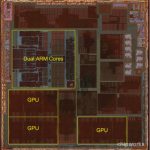
With the launch of the iphone 5 behind him and the supply chain ramped to deliver 50MU of iPhone 5 in Q4, there seems to be a silly game in the press of how to raise Tim’s dander on all that is wrong in the Apple ecosphere. The component shortages that exist today are in reality the flip side of the coin known as unlimited demand at Day 1 of the new product launch. However, with Samsung ever on Apple’s heals, the game doesn’t stop and Apple must continue to innovate as well as wring out supply chain inefficiencies. The one that, no doubt, is staring Cook in the eye for 2013 is the A6 processor currently in production in Samsung’s Austin Fab. It is the last major component being produced by Samsung and it needs to move to a friendlier foundry.
For months the rumor mills have been rattling with stories of a TSMC – Apple partnership at 20nm targeting first production the end of 2013. This seems logical, given that Apple is moving to a two-supplier model across most of its major components. If they were to continue with this strategy, then it would mean they have to pick up another foundry (i.e. Global Foundries or Intel) to go hand in hand with TSMC and avoid any single point of failure due to “Acts of God” or unforeseen upside, both of which we have seen the past 24 months.
Intel’s announcement a couple weeks ago on a PC slowdown in Q3 came with a hint that 22nm is yielding well. If, however Intel’s revenues going forward are flat or even slightly rising as opposed to the 24% growth they experienced in both 2010 and 2011 then the Fab expansion plans they outlined last year regarding 22nm and 14nm would raise the question – for what reason? Perhaps it was the only strategy that Otellini could logically employ as Intel tries to outrun TSMC and Samsung.
A year ago, there were doubts as to whether Intel’s new 22nm Finfet process would yield as well as previous process technologies. If the PC market and the DataCenter continued to grow as in past years and if Ivy Bridge were to cannibalize the graphics cores of AMD and nVidia, then the argument could be made to expand Intel’s 22nm Fab footprint from 3 to 4. And so it is expected at year-end the 4[SUP]th[/SUP] Fab will come on line while Intel is swimming in well yielding Ivy Bridges. Look out below AMD and nVidia, your days may be numbered in a soft PC market.
The addition of two mammoth 14nm Fabs that can be upgraded to 450mm to Intel’s capex budgets seems to speak of insanity, unless they expect them to come on line much sooner and that it truly does represent a 4 year lead over competitors. Mark Bohr at IDF mentioned that 14nm will be ready for production the end of 2013 and word is that the 14nm successor to Haswell, called Broadwell, is already up and running Windows. This begs the question, is Broadwell really two years away from production or will Intel launch it early, thus setting up a 22nm to 14nm Fab transition 2H 2013? Otellini would seem to be in a position to deploy his large, highly efficient 22nm Aircraft Carriers in any number of Foreign Oceans wreaking havoc. Or perhaps, aggressively leverage them for a long-term fab deal with Apple.
If Otellini were to offer Apple free wafers, would Tim Cook disregard it? Preposterous you say. OK, but this is what game theory is all about. You have to test the limits and I believe until the summer slowdown, Otellini’s bid to Apple was to sell wafers with a 60% margin markup.
In this new environment, Otellini will be more likely to offer a price that is closer to cost plus a small adder for anytime starting first half 2013 and extending thru 2015. What are the ramifications for Apple? The new A6 processor is a 95mm die in Samsung’s 32nm process and costs somewhere around $25 (I have seen estimates from $18 to $28). In round numbers the A6 in Intel’s 22nm process is 50mm in size. If Intel saves Apple $10 a chip, then it is equivalent to $3B a year (300MU) that drops to its Operating line and would add nearly $50 to Apple’s stock price (based on 15.5 P/E).
The overriding issue for Intel and Paul Otellini is, as I mentioned before, that they need to move to 14nm as quickly as possible and take as much of the market with them (both x86 and Apple) and thereby eliminate the threat posed by TSMC and Samsung as Foundries looking to supply a greater percentage of the total semiconductor market that is built in leading edge processes. Until the last couple years, Intel consistently had over 90% of the leading edge compute semiconductor content delivered with their x86 processors, a legacy that goes back to the transition of IBM mainframes to the Desktop PC.
The End Game continues to get more interesting as we get closer to “All In with Leading Edge.”
Full Disclosure: I am Long AAPL, INTC, QCOM and ALTR