Let’s play word association. I say “EDA”, you immediately think “Synopsys”. I say “IP” and although 15 years ago you may not, today, you think “Synopsys”. For nearly two decades, Synopsys has grown its IP business through both organic development and acquisition, with a clear focus on enabling designers to meet their time-to-market requirements and reduce integration risk by providing the high-quality IP they need, precisely when they need it.
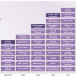
Today, Synopsys is considered by designers as the industry’s trusted IP partner. Its DesignWare IP is shipping in billions of chips … and counting. According to the latest research from Gartner, Synopsys is the leading provider of interface, analog and memory IP and the No. 2 provider of IP in the industry. In 2012 Synopsys achieved its 100th design win with its 28-nanometer (nm) IP and was awarded TSMC’s 2012 Interface IP Partner of the Year for the third consecutive year. These milestones, along with more than 1400 engineers and a worldwide technical support team demonstrate Synopsys’ commitment to helping customers achieve their design goals at every step. The world of IP is definitely changing. With the shift to IP subsystems, 20-nm IP and FinFET, Synopsys remains in the forefront of providing the IP needed for these technology advancements. Figure 1: Synopsys’ Growing IP Business:
So How Did Synopsys Get Here?
In the 1990s Synopsys launched the DesignWare Foundation Library, a collection of technology-independent, reusable building block IP such as adders and multipliers that are tightly integrated with Synopsys’ synthesis environment, delivering significant improvements in area, timing and runtime. Through the years, complex IP blocks were added to the library such as 8-bit microcontrollers, AMBA on-chip bus IP as well as verification IP (a.k.a. SmartModels). With these additions, the product became known as the DesignWare Library – and it has been the most widely used library of foundation IP ever since.
Fast forward a decade. We saw an explosion in the usage of standards-based communication protocols, setting the stage for the emergence of the commercial IP industry as companies realized they needed to focus their efforts on the differentiated portions of their design and not on developing standards-based IP. In 2002, Synopsys acquired inSilicon, adding popular interface protocols such as PCI-X, USB, IEEE 1394 and JPEG to its DesignWare IP portfolio. By 2004, Synopsys was seeing increased demand in PCI Express (PCIe) for data center and server applications. By acquiring Cascade Semiconductor, Synopsys rounded out its already successful DesignWare PCI Express Endpoint solution with root port, dual mode and switch ports, providing designers with a complete high-performance, low-latency PCI Express IP solution. Also in 2004, the acquisition of Accelerant Networks brought serializer-deserializer (SerDes) technology to Synopsys. Figure 2: DesignWare PCI Express IP Solution:
In 2007, Synopsys released the DesignWare USB 2.0 nanoPHY, its next-generation USB 2.0 PHY, which cut the power and size in half over the previous generation. The expansion of Synopsys’ IP portfolio continued that year with the launch of digital controllers for PCI Express 2.0 (5.0 GT/s), mobile storage, SATA AHCI and the acquisition of Mosaid’s DDR memory controllers and PHY IP. One year later, Synopsys continued its momentum in DDR by releasing a full range of silicon-proven DDR3 and DDR2 IP solutions and announced a complete SuperSpeed USB 3.0 IP solution.
In 2009, Synopsys moved into the analog IP business with the acquisition of the Analog Business Group of MIPS Technologies. The acquisition added to the DesignWare IP portfolio a new family of analog IP such as analog-to-digital converters (ADCs), digital-to-analog converters (DACs) and audio codecs. It also added HDMI 1.3 transmitter (Tx) and receiver (Rx) IP to Synopsys’ existing interface portfolio. With this acquisition, designers were able to go to a single, trusted vendor for both their analog and interface IP needs. In the same year, Synopsys introduced new products such as minPower Components; Ethernet IP with support for the IEEE 1588 specification; DDR3 IP operating at 2133 Mbps data rate and 1.35V DDR3L, SATA 6 Gbps digital controllers; and a complete solution for PCI Express 3.0 (8.0 GT/s).
The acquisition of Virage Logic in 2009 added logic libraries and embedded memories, enabling designers to achieve the best combination of power, performance and yield; memory test and repair; non-volatile memory; and ARC processors targeted at embedded and deeply embedded applications. Throughout 2010, Synopsys continued to introduce new products that would help designers integrate advanced functionality into their SoCs such as:
- Third -generation USB 2.0 PHY – the USB 2.0 picoPHY (30% smaller area and lower power compared to the previous generation)
- 40-nm data converters
- Universal DDR controllers supporting DDR2, DDR3, Mobile DDR and LPDDR2 standards
- DDR multiPHY supporting six DDR standards
- MIPI 3G DigRF, DigRF v4, CSI-2 controller, DSI host controller and D-PHY
- HDMI 1.4 Tx/Rx controller and PHY
- Ethernet controller with an audio-video bridging feature
- DesignWare STAR ECC (error-correcting codes)
- ARC processor cores for Blu-ray Disc players
In 2011, the focus was on helping designers develop 28-nm SoCs. Synopsys announced the availability of DesignWare Interface PHY and Embedded Memory IP for TSMC’s advanced 28-nm process as well as the collaboration with UMC on embedded memory and logic library in 28-nm. Significant milestones were also achieved, including Synopsys’ DesignWare STAR Memory System being shipped in one billion chips, DesignWare SuperSpeed USB 3.0 IP achieving more than 40 design wins, and GUC taping out 30 customer chips using DesignWare IP. The DesignWare ARC EM processor family for embedded applications was also launched this year.
In 2012, designers started to integrate more and larger third-party IP into SoCs, it wasn’t enough to just provide individual IP blocks – the market needed complete IP subsystems to ease the integration effort. In March 2012, Synopsys unveiled the industry’s first complete, pre-integrated and configurable audio subsystem consisting of hardware, software and prototyping. Figure 3: DesignWare SoundWave Audio Subsystem:
In the same year, Synopsys also had significant IP product releases such as the industry’s first 28-nm Multi-Gear MIPI M-PHY IP supporting six standards, DDR4 memory controller and PHY, MIPI UniPro and UFS, STAR Memory System for 20-nm designs and IP for the SMIC 40-nm low leakage process.
With more functionality going into a single device, third-party IP continues help designers reduce risk and speed time-to-market. Based on Synopsys user surveys, the top five criteria for selecting an IP provider are:
[LIST=1]
- IP technology leadership
- Quality/silicon-proven IP
- Market leadership
- Brand reputation, and
- Breadth of IP portfolioThese have been Synopsys’ IP priorities as well.To learn about all the DesignWare IP developments, visit the website.