FinFETs are hot, carbon nanotubes are cool, and collaboration is the key to continued semiconductor scaling. These were the main messages at the 2013 Common Platform Technology Forum in Santa Clara.
The collaboration message ran through most presenations, like the afternoon talk by Subi Kengeri of GLOBALFOUNDRIES and Joe Sawicki of Mentor Graphics.
Subi talked about technology development, identifying the market drivers of technology (mobile), the technology challenges (power density, metrology for FinFETs), and the future device architectures (III-V, SiGe, carbon tube). Listening to him lay out the technology landscape, one starts to understand why cooperation between Common Platform Alliance members (IBM, Samsung, GlobalFoundries) is so important.
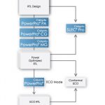
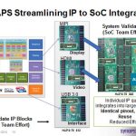
While the industry was once full of vertically integrated semiconductor companies who could conceive of, design, and manufacture their ICs under one roof (“real men have fabs”), today, the fabless semiconductor industry depends on the “ecosystem” of IP, EDA, manufacturing, test and packaging. The EDA part of the equation, design enablement and manufacturing ramp, was covered by Joe Sawicki.
Joe emphasized that DFM today involves pulling manufacturing knowledge into the design flow as early as possible. Mentor is keenly aware of the importance of manufacturing on all stages of design, so much so that they built a new website focused on foundry solutions.
To get a manufacturable design, you have to go far beyond simply reading in a technology file with basic spacing rules. You need enough information flowing between tools for a true design/manufacturing co-optimization. From the EDA point of view, this means merging physical verification with place & route (Calibre InRoute), fusing DFM with test and yield analysis, streamlining final verification (pattern matching, DFM scoring), improving metal fill, developing technologies to improve circuit reliability (PERC), and improving test coverage for low- or 0-defect applications (cell-aware ATPG). It begins to look as if the nice, distinct boxes of the IC design flow are escaping their boundaries, blending together. Is it chaos? Is it cats and dogs living together? No, it’s the future; everything working better through mashups and collaborations.
In fact, my analysis of word usage in the day’s presenatations revealed that “collaboration” was the most frequently used term of the day. Keep in mind that this reporter’s analysis is based on general recollections during happy hour, but still, I stand by it.