It has be come a cliche to say that “power is the new timing”, the thing that keeps designers up at night and drives the major architectural decisions in big SoCs. Nobody is saying it yet but perhaps “reliability is the new power” will be tomorrow’s received wisdom.
I talked to Adrian Evans of IROCTech last week. He used to work at Cisco and with an enormous installed base of routers processing enormous amounts of data, very rare events such as Single Event Effects (SEE) happen all the time. And customers don’t like it when their routers reboot for no discernible reason, not to mention being very expensive for Cisco to swap out “faulty” boards that actually have no faults, just got hit by a random cosmic ray. The chips in those generations of routers are not even 28nm or 20nm, and SEE problems get worse with process generation, as the gate-oxide becomes just a few atoms thick, the power densities increase and lower voltages lead to lower noise margins. So one thing you will see is system companies such as Cisco specifying reliability standards for all chips.
Several years ago, when power really started to become the huge issue it is today, we developed power standards. Of course purchasers of chips would specify power numbers, especially for mobile devices, but the place that power really changed design was in building power delivery networks (and analyzing them), board design and a standard file format. Well, we are EDA, so we can never make do with one standard when two would be more fun, so we ended up with both CPF and UPF with broadly comparable capabilities as a way of specifying power policy throughout the design flow.
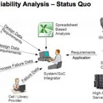
There is no equivalent format for specifying reliability data, constraints, policy etc throughout the design flow. You can go into PrimeTime and say “report_timing” or “report_power” but “report_reliability” won’t give you anything.
Like other things in design, reliability is a tradeoff. For chips in satellites, triple redundancy and voting might be appropriate to achieve extremely high levels of reliability in an extremely difficult environment, but it would be completely inappropriate for a cell-phone. In other environments, errors in the chip may not be so important if they can be detected and corrected in software. You can see that reliability is thus a chain from software down to chips down to things like making sure the solder in your package doesn’t emit too many alpha particles. As with any chain, it is only as strong as the weakest link. But the corollary is that there is no point in building one or two especially strong and expensive links, you want all the links to be roughly the same strength.
We are past the time at which spreadsheets and email work as a way of passing reliability data around. What is required is a Reliability Information Interchange Format (RIIF). Well, such a standard is, in fact, in development. It is a modeling language with a purpose to specify the rate of occurrence of failure modes in electronic components. The goal is to make it an eventual IEEE standard. Work started about a year ago, largely in conjunction with the European automotive manufacturers.
People expect their cars to last 10 or 20 years and much of the electronics in cars has to work in a fairly hostile environment, climbing out of death valley in summer means that the ECUs in the car are in a very hot environment, Minnesota in February not so much. And the electronics in cars (now well over 100 electronic control units or ECUs are in a high-end car) is, in many cases, safety critical. For sure, Cisco doesn’t want their routers to reboot unexpectedly. But you really don’t want your ABS system to reboot unexpectedly. So the automotive manufacturers are in the vanguard of driving reliability metrics down their supply chain.
There are two important workshops on this topic coming up this month, one in Silicon Valley and one in Europe in Grenoble:
- Silicon Errors in Logic – System Effects (SELSE) at Stanford, March 26th and 27th. Details here. Keynotes from Microsoft, IBM and DoD CEC.
- 1st RIIF Workshop, Grenoble, March 22nd (co-located with DATE). Towards Standards for Specifying and Modeling the Reliability of Complex Electronic Sytems. Details here. There are speakers from ARM, Intel, Bosch, Infineon Automotive among others.