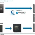
Edmond Macaluso, President of Z-Circuit Automation met with me at DAC on Tuesday afternoon to provide an overview of how their EDA tools characterize cell libraries. Continue reading “IC Cell Library Characterization at DAC”
Mike Muller’s ARM Keynote at DAC 2012
Mike Muller’s keynote focused on a lot of changes since the ARM1 was designed in 1983 when ARM the company did not exist and ARM was the next generation processor for Acorn Computer, which was really in the hobby market and had its first boost when they had a contract to design the BBC Microcomputer to go along with a computer literacy project. My minor claim to fame about the ARM1 was that I installed the VLSI Technology design software that was used to design it on two Apollo workstations (which hadn’t actually shipped so I had to go and install it at Apollo not Acorn).
Mike decided to dig up the layout of the ARM1, which turned out to be more of a challenge than expected, involving finding an Exabyte drive, converting VAX files to Linux and converting from CIF (which VLSI Technology used for layout) to GDSII. The original ARMs were full custom designs (this predated synthesis). ARM have recently announced a low end microcontroller, the Cortex-M0. It turns out that this is roughly the same number of transistors as the ARM1 so it makes an interesting basis for comparison.
The chips are about 26 years apart, or 13 process generations, so it should be about 1/2[SUP]13[/SUP] smaller (namely 1/8000) and it is actually 1/10,000 times smaller so about right. Performance should be about 6 performance scalings, so 64 times as fast but it is only 16 times as fast. This is because the 5V power supply that the ARM1 used should have scaled down to 8mV but in fact it has only scaled to 950mV and so the transistor threshold voltages haven’t scaled enough.
The big change in design is that the ARM1 took 6 months to layout. The Cortex-M0 took 32 minutes. Basically synthesis, place and route has automated the whole process whereas the ARM1 was custom. But that is really the only major improvement in design methodology.
Mike then looked at the design productivity. The ARM1 took 6 man-years (MY) and was 25,000 transistors. The dual Cortex-A15 took 150MY and is 150 million transistors. Luckily design productivity has increased 240 times. It is when you look at software that things are scary. The ARM1 graphics library was 0.25MY of work and was 150 lines of code (Loc). Assembly of course. The current ARM GPU, the Mali-T604 has OpenGl, open CL and other graphics support and is 190MY of work and 1M LoC. Just a 7 times increase in productivity.
Mike pointed out that the hardware people shouldn’t be complacent. We came up with synthesis and P&R so that we can essentially compile our chips. But we haven’t come up with anything comparable since. Software people have moved onto Python, cloud computing, development environment and lots of new goodies. So apart from the few people left having to write device drivers, the way software is being developed is changing fast.
Next Mike moved onto validation. The ARM1 was in 3um, had 24,000 transistors and took 6 MY to validate. The Cortex-M0 is in 20nm, 32,000 transistors (not much more) and took 11 MY to validate. But the big difference is the machine resources brought to bear. The ARM1 took 2,000 hours to validate but the Cortex-M0 took 1,439,000 hours to validate. Taking the speed of the machines into account this is 3,000,000 times less efficient. We waste a lot of computer cycles early, especially with constrained random verification, in order to avoid silicon respins later.
Mike feels we need to get more formal design techniques. Today formal verification is stuck on the side of the design process as an “optional extra” to be run by a specialist, rather than something embedded deeply in the design process. Without this we are stuck with constrained random and burning computer and verification engineer cycles, and formal verification not part of every designers job.
As an aside, Mike talked a bit about building ARM’s datacenter in the parking lot. It has 200TFLOPS and 93TB DRAM. It consumes 1.5MW (luckily there was a new housing tract going in across the street so they actually managed to get a line like that installed). The UPS consists of two parts, firstly 6 spinning flywheels which can each deliver 250KW for 20 seconds. Then two 785bhp quad turbo diesel generators that can get up to full power in 8 seconds. Looks pretty good too!
There is a video the keynote here. The video starts with the DAC award session and the keynote itself starts at 29 minutes in. Wait and let enough of the video load and then you can skip straight to the start (unless you really want to see a re-run of the award session).
Off topic: Matt
This has pretty much nothing to do with EDA or semiconductor. OK, absolutely nothing. Years ago a friend pointed me at a video of a guy who used to be a video game designer (wait, a semiconductor connection) who decided to take his savings and travel the world. As he put it, “I wasn’t a very good video game designer. But I was good at travel.” He filmed himself dancing badly in front of famous places, put them together into a video and it went viral. A chewing gum company sponsored him to make two more, equally successful. Visa and hotels.com paid him to make ads…
I was at TED in Palm Springs three years ago (the TED for people who are too poor and not nearly famous enough to go to the real one) and he was there for one of the token events that was live in Palm Springs and everyone in Long Beach had to watch on video feed. I talked to him at the party that evening. He said he was trying to travel less since he had a girlfriend so couldn’t just live on the road for months on end. But she became the producer and the story carried on.
Anyway, after two years in the making, the 2012 video was released today. It’s a huge undertaking when you compare it to the first original one. I suspect this will be the last one for some time. You’ll see why when you see him dancing in Seattle (his home town) in the last scene.
I don’t understand YouTube statistics: 7000 people already “like” it, 2000 people have commented, but apparently only 301 have seen the video.
Enjoy.
Double Patterning Technology at DAC
David Abercrombie from Mentor Graphics met with me on Tuesday at DAC to provide an update on DPT – Double Patterning Technology, something new required for several layers starting at the 20nm node in order to get any IC yield. DPT is also part of Multiple-Patterning. Continue reading “Double Patterning Technology at DAC”
Custom IC Layout Automation at DAC
Three people from Ciranova met with me at DAC this year: Eric Filseth (CEO), David Millman (Marketing) and Lindor Hendrickson (CTO). They gave me an update on how the Helix tools are being used to automate the layout of custom IC designs at 28nm and smaller nodes. Continue reading “Custom IC Layout Automation at DAC”
IPL Alliance at DAC
Lunch on Tuesday at DAC was sponsored by the IPL Alliance and thankfully this year they skipped the attempt at humor and focused on interoperable PDKs. Presenting companies include: Synopsys, Dongbu HiTek, TowerJazz, X-FAB and Si2. Having both OpenPDK and iPDK on the same platform does sound like a peaceful co-existence to me, although I wasn’t too sure about that one year ago.
Tensilica: We are #2 so we try harder
The Linley group is the go-to source for information about the microprocessor market. If you go back to their roots in Michael Slater’s Microprocessor Report then they have been in the business for 25 years. We haven’t had microprocessors for that much longer. They just tagged Tensilica as being second in shipments of chips containing DSP cores. Last month Linley published numbers showing CEVA as #1 but, as I blogged about, they classified Tensilica and ARC as general purpose cores and didn’t include them in the DSP market. They have since reconsidered that position since, in fact, many Tensilica cores are used for audio, video and cellular (e.g. LTE) signal processing. For example, Tensilica is in the Audience chips in the iPhone. Linley now reckon that 1.5 billion chips were shipped in 2011 with licensable DSP cores and Tensilica is 20% of that market (so that would be about 300M DSP cores). Tensilica say that shipments of cores roughly doubled in 2011 from 2010.
Last year Tensilica announced that their licensees had cumulatively shipped over one billion Tensilica cores and they expect to pass two billion (cumulative) by the end of 2012. So roughly a billion Tensilica cores shipped during 2012, that’s impressive growth. Of course it is the nature of the IP business that you license a core and then…nothing happens. The chip has to be designed, prototyped, designed into a product, ramped to volume and only then do royalties flow (and you get on Linley’s radar).
As Mike Muller of ARM said to me years ago, “royalties always come later than you expect and are less than you expect.” When you are a big supplier, one reason is that some of your accounts will be big hits and some will not, but they all gave you optimistic predictions of the volumes they hoped to ship. For every iPhone that takes off like a rocket there is a Blackberry or a Lumia that isn’t selling because…well, everyone is buying iPhones. I remember in the early days of VLSI Technology when the PC business was taking off, we had about a dozen customers designing PC ASICs of one sort or another with a business strategy of being 25% of the PC market. We had no idea which ones would succeed but for sure not all of them. The answer pretty much turned out to be none of them.
Oh, and if you are visiting Tensilica they are about to move. But you are in the right place. They will be moving to the two storey building just across the street.
Totally off-topic, there is an interesting story behind the Avis tagline that I used as the title to this blog, as told in Robert Townsend’s book Further Up The Organization. Townsend went to his advertising agency DDB and asked the head how he could effectively get $2 of advertising for every $1 he spent, since Hertz was twice his size. He was told “just do this: promise that you you will not nitpick, that you will run whatever ad you select completely unchanged. you will have every person in this office moonlighting on your account.” After a couple of months DDB went back to Avis and told them that the best they had come up with was the “we’re #2 so we try harder” idea. Nobody seemed that keen on it but Townsend had promised to run the ads unchanged, so they did. The rest is history and it is now one of the most recognized taglines ever.
Atrenta Aquires NextOp
Atrenta announced today that it is acquiring NextOp Software. NextOp sells a tool BugScope that provides assertion synthesis technology. This complements Atrenta’s SpyGlass products for improving the process for design of complex semiconductor IP and SoCs.
I went to Atrenta’s office to talk to Ajoy Bose (CEO) and Mike Gianfagna (VP marketing).
It’s not been a secret that Atrenta has been looking to do an acquisition, but one challenge being as large as they are is that it has to be a reasonable sized acquisition to make any difference. NextOp is a private company with no institutional investors. It is a couple of dozen people, half in San Jose (who will move into Atrenta’s building) and half in Shanghai (which will create a fifth R&D center for Atrenta, along with San Jose, India, Grenoble and, most recently, Sri Lanka where they have 20 people going to 30 by the end of the year).
Of course the other big aspect of an acquisition is that it should be synergistic with Atrenta’s existing business, not just be a bit of additional revenue. That is it should be more than additive and drive growth too. NextOp fits the bill. It is a good sized business with good momentum and the Atrenta channel should be able to start selling the product immediately into their 200-odd customers (NextOp has about a dozen customers including Altera, AMD, IDT, PLX and nVidia. They are mostly already Atrenta customers too).
NextOp seems to do for functional verification what Atrenta does for synthesis, static timing, place and route and so on. That is they don’t do any of those things but they make the whole process smoother and more effective, thus reducing cost, time-to-market and improving quality. NextOp looks at the results of simulations and generates assertions and functional coverage properties which can be used with simulation, emulation and formal verification to improve overall verification. They call this assertion synthesis.
NextOp will make a nice addition to IPKit too, which today encompasses a lot of factors like waivers that make flows based around integrating IP smoother. Now this can be expanded to include assertion and functional coverage properties, which was previously a hole in Atrenta’s offering.
Financial details of the transaction were not disclosed. Both companies are private and it took several months of negotiations to reach a deal (two companies with currency that nobody really has a good valuation for must make for some interesting discussions).
Shape-based IC Routing at DAC
IC place and route is a big challenge so we see many EDA companies creating tools. On Tuesday at DAC I met with Dave Noble of Pulsic to get an update.
Notes
Dave Noble, VP Operations (EDA since 2003), Sperry Univac since 1974
– had been an EDA distributor for Pulsic as well
More leads qualified on Monday than all days of last year at DAC.
What’s new this year?
History
12 years old, technology from Zuken, a shape-based router with Japanese customers. Toshiba and Renesas steered the company to do analog routing. A tool to complement the skills of an IC layout designer, not replacing their job.
Take a 6 week manual route into one day, you still have to control the process. Automation or interactive routing, it’s your choice.
SHort learning curve by designs, easy to setup constraints, not a week long learning. Own GUI, not an integration into Cadence GUI. ROuting can be exported to OA.
Unity CUstom Digital Router – been around for 12 years now. Has STA built in to the tool flow, so you don’t have to exit the router to understanding timing impact.
Unity Analog Router – new this year. Not as automated as CiraNova, more intuitive to your existing analog flow. Constraints are annotated in the schematic. We distinquish between custom and analog IC layout. Analog centric routing. Online DRC by reading a Cadence deck.
– Could read a Calibre deck, but not there yet. TSMC has about 10 pages of rules for analog routing. Goal is DRC correct by design, also you can check and fix in a semi-automated fashion.
– Pyxis was a litho-aware router.
– Virtuoso : Custom router with some analog features.
– CiraNOva: Press the route button and hope for the best, but didn’t get what I wanted.
Unity Bus Planner – separate piece available.
CUstomers: Samsung, Micron, (DRAM, Flash, PCM). AMS companies in Japan and US, FPGA. Memory companies like the sophisticated shape-based approach for routing the IO. Network switching companies starting to use Pulsic routers.
Shape-based isn’t constrained to a grid, so results are more efficient with fewer jogs and vias. Not aimed at being an ASIC router company.
Reference flows at Foundry – most of our clients are IDMs so we aren’t qualified at TSMC and other foundries. Do have customers using 28nm at TSMC.
Development in the UK (Bristol, New Castle), Japan.
Privately held and funded. Growth plans – add analog routing. 2011 about 30% growth and 2012 about 25% growth. Hiring now.
Time based licenses, typically 3 years, including support and training.
Why you versus competitors? Manual routing is the primary competitor.
Evaluations: Used to be 9 months, now about 6 months. Set a criteria of success.
Any consulting services? Yes, we do some of that for our customers in terms of creating and optimizing a flow, working with their data.
3rd party: Cadence Connections, Mentor OPen Door, Synopsys inSync, SpringSoft.
12 months from now – continued revenue growth, more people (32 now), new products next year from internal development. Enough cash to last 3 years, so have conservative growth plans.
Japan – distributor is Jedat.
Release cycles – green build every 3 months, SCRUM methodology. Customers can track the progress of every bug filed, complete transparency.
Summary
Pulsic offers P&R tools for both digital and analog IC designers. They compete in a crowded market with: Cadence, Synposys (Magma), Mentor and A Toptech.
3D Thermal and Mechanical Stress for IC Packaging
3D has been a growing buzz word in IC design and packaging for several years now, so it’s refreshing to actually find an EDA vendor that has developed tools to help analyze something like 3D thermal and mechanical stress at DAC. Continue reading “3D Thermal and Mechanical Stress for IC Packaging”