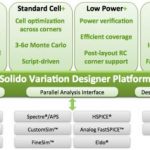
SMT webinar banner3

ARM + Broadcom + Linux = Raspberry Pi

ARM + Broadcom + Linux = Raspberry Pi
by Daniel Payne on 08-23-2012 at 12:28 am

Broadcom has designed an impressive SOC named the BCM2835 with the following integrated features:

  • ARM CPU at 700MHz
  • GPU – VideoCore IV
  • RAM – 256 MB

The British chaps at Raspberry Pi have created a $35.00 Linux-based computer based on the Broadcom BCM2835 chip that is tiny in size but big in utility: Continue reading “ARM + Broadcom + Linux = Raspberry Pi”


Debugging Subtle Cache Problems

Debugging Subtle Cache Problems
by Paul McLellan on 08-22-2012 at 5:11 pm

When I worked for virtual platform companies, one of the things that I used to tell prospective customers was that virtual prototypes were not some second-rate approach to software and hardware development to be dropped the moment real silicon was available, that in many ways they were better than the real hardware since they had so much better controllability and observability. An interesting blog entry on Carbon’s website really shows this strongly.

A customer was having a problem with cache corruption while booting Linux on an ARM-based platform. They had hardware but they couldn’t freeze the system at the exact moment cache corruption occurred and since they couldn’t really have enough visibility anyway, they had not been able to find the root problem. Instead they had managed to find a software workaround that at least got the system booted.

Carbon worked with the customer to put together a virtual platform of the system. They produced a model of the processor using Carbon IP Exchange (and note, this did not require the customer to have detailed knowledge of the processor RTL). They omitted all the peripherals not needed for the boot (and also didn’t need to run any driver initialization code, speeding and simplifying things). Presumably the problem was somewhere in the memory subsystem. There was RTL for the L2 Cache, AHB fabric, boot ROM, memory controller, and parts of their internal register/bus structure. This was all compiled with Carbon Model Studio to a 100% accurate model that could be dropped into the platform. And when they booted the virtual platform the cache problem indeed showed up. When you are having a debugging party it is always nice when the guest of honor deigns to show up. Nothing is worse than trying to fix a Heisenbug, where when you add instrumentation to isolate it the problem goes away.By analyzing waveforms on the ARM High-performance Bus (AHB), the cache-memory, the memory controller, and assembly code (all views that Carbon’s SOCDesigner provides) they isolated the problem. It turned out that the immediate problem was that a read was taking place from memory before the write to that memory location had been flushed from the cache, thus picking up the wrong value. In turn, the real reason was that a writethrough to the cache (which should write the cache and also write through to main memory) had been wrongly implemented as a writeback (which just goes to the cache immediately and only gets written to main memory when that line in the cache is flushed). With that knowledge it was easy to fix the problem.

They had not been able to fix this problem using real hardware because they couldn’t see enough of the hardware/software interaction, bus transactions and so forth. But with a virtual platform, where the system can be run with fine granularity, complete accuracy and with full visibility, this type of bug can be tracked down. As Eric Raymond said about open source, “with enough eyeballs, all bugs are shallow.” Well, with enough visibility all bugs are shallow too.Read more detail about this story on the Carbon blog here.


Synopsys up to $1.75B

Synopsys up to $1.75B
by Paul McLellan on 08-22-2012 at 4:24 pm

Synopsys announced their results today. With Magma rolled in (but not yet SpringSoft since that hasn’t technically closed) they had revenue of $443M up 15% from $387M last year. This means that they are all but a $1.75B company and a large part of the entire EDA industry (which I think of as being $5B or so, depending on just what you do about services, IP, ARM in particular etc). GAAP earnings per share were $0.50 (non-GAAP was $0.55). GAAP (which stands for generally accepted accounting principles excludes various deductions especially in the way acquisitions are accounted and stock compensation is accounted).

For their fourth quarter they expect revenue to be flat versus this quarter at $440-448 million. So for fiscal 2012 (which ends in October) they expect revenue of $1.74 to $1.75B, with positive cash flow for the year of $450M. If Synopsys manage to grow another 15% next year (either through organic growth or through acquisition, and presumably SpringSoft is already in the bag) then they will be over $2B a year running roughly $500M/quarter, which I think is an amazing achievement given that Synopsys in 2000 was $784M, which it now takes just 5 months to do.

And, talking of acquisitions, it still has close to $1B in cash. The one area where Synopsys is weak is emulation so I wouldn’t be the least bit surprised to see them go after Eve.

Full press release including P&L, balance sheet etc is here.


Cadence at 20nm

Cadence at 20nm
by Paul McLellan on 08-21-2012 at 8:10 pm

Cadence has a new white paper out about the changes in IC design that are coming at 20nm. One thing is very clear: 20nm is not simply “more of the same”. All design, from basic standard cells up to huge SoCs has several new challenges to go along with all the old ones that we had at 45nm and 28nm.

I should emphasize that the paper is really about the problems of 20nm design and not a sales pitch for Cadence. I could be wrong but I don’t think it mentions a single Cadence tool. You don’t need to be a Cadence customer to profit from reading it.

The biggest change, and the one that everyone has heard the most about, is double patterning. This means that for those layers that are double patterned (the fine pitch ones) two masks are required. Half the polygons on the layer go on one mask and the other half on the other mask. The challenge is that no patterns on either mask can be too close, and so during design the tools need to ensure that it is always possible to divide the polygons into two sets (so, for example, you can never have three polygons that are minimum distance from each other at any point, since there is no way to split them legally into two). Since this is algorithmically a graph-coloring problem this is often referred to as coloring the polygons.

Place and route obviously needs to be double pattern aware and not create routing structures that are not manufacturable. Less obvious is that even if standard cells are double pattern legal, when they are placed next to each other they may cause issues between polygons internal to the cells.

Some layers at 20nm will require 3 masks, two to lay down the double patterned grid and then a third “cut mask” to split up some of the patterns in a way that wouldn’t have been possible to manufacture otherwise.

Another issue with double patterning is that most patterning is not self-aligned, meaning that there is variation between polygons on the two masks that is greater than the variation between two polygons on the same mask (which are self-aligned by definition). This means that verification tools need to be aware of the patterning and, in some cases, designers need to be given tools to assign polygons to masks where it is important that they end up on the same mask.

Design rules at 20nm are incredibly complicated. Cadence reckon that of 5,000 design rules only 30-40 are for double patterning. There are layout direction orientation rules, and even voltage dependent design rules. Early experience of people I’ve talked to is that the design rule are now beyond human comprehension and you need to have the DRC running essentially continuously while doing layout.

The other big issue with 20nm are layout dependent effects (LDEs). The peformance of a transistor or a gate no longer depends just on its layout in isolation but also on what is near it. Almost every line on the layout such as the edge of a well has some non local effect on the silicon causing performance changes in active areas nearby. At 20nm the performance can vary by as much as 30% depending on the layout context.

A major cause of LDEs is mechanical stress. Traditionally this was addressed by guardbanding critical paths but at 20nm this will cause too much performance loss and instead all physical design and analysis tools will need to be LDE aware.

Of course in addition to these two big new issues (double patterning, LDEs) there are all the old issues that just get worse, whether design complexity, clock tree synthesis and so on.

Based on numbers from Handel Jones’s IBS, 20nm fabs will cost from $4-7B (depending on capacity), process R&D will be $2.1-3B on top of that, and mask costs will range from $5-8M per design. And design costs: $120-500M. You’d better want a lot of die when you get to production.

Download the Cadence white paper here.


A Brief History of ASIC, part I

A Brief History of ASIC, part I
by Paul McLellan on 08-21-2012 at 7:00 pm

In the early 1980s the ideas and infrastructure for what would eventually be called ASIC started to come together. Semiconductor technology had reached the point that a useful number of transistors could be put onto a chip. But unlike earlier, when a chip only held a few transistors and thus could be used to create basic generic building blocks useful for everyone, each customer wanted something different on their chip. This was something the traditional semiconductor companies were not equipped to provide. Their model was to imagine what the market needed, create it, manufacture it and then sell it on the open market to multiple customers.

The other problem was that semiconductor companies knew lots about semiconductors, obviously, but didn’t have system knowledge. The system companies, on the other hand, knew just what they wanted to build but didn’t have enough semiconductor knowledge to create their own chips and didn’t really have a means to manufacture those chips even if they did. What was required was a new way of doing chip design. The early part of the design, which was system knowledge heavy, would be done by the system companies. And the later part of the design, which was semiconductor knowledge heavy, would be done by the company that was going to manufacture it.

Two companies in particular, VLSI Technology and LSI Logic, pioneered this. They were startup companies with their own fabs (try getting that funded today) with a business model that they would, largely, build other people’s chips. In the early days, since there weren’t really any chips out there to be built, they had to find other revenue streams. VLSI Technology, for example, made almost all of its money building read-only-memories (ROMs) that went into the cartridges for the first generation of video game consoles.

Daisy, Mentor and Valid, who had electronic design systems mostly targeted at printed circuit boards, realized that they could use those systems for the front end of ASIC design too.

ASIC design typically worked like this. A system company, typically someone building an add-on board for the PC market since that was the big driver of electronics in that era, would come up with some idea for a chip. They would negotiate with several ASIC companies to decide which to select, although it was always a slightly odd negotiation since only a vague idea of the size of the design was available at that point. They would then partner with one ASIC company such as LSI Logic who would supply them with a library of basic building blocks called cells.

The system company would use a software tool called a schematic editor to create the design, picking the cells they wanted from the library and deciding how they should be connected up. The output from this process is called a netlist, essentially a list of cells and connections.

Just like writing software or writing a book, the first draft of the design would be full of errors. But with semiconductor technology it isn’t possible to build the part and see what the errors are. Even back then it cost tens of thousands of dollars and a couple of months to manufacture the first chip, known as the prototype. Also, unlike with writing a book, it’s not possible to simply proofread it and inspect the schematic, too many errors would still slip through.

Instead, a program called a simulator was used. A flight simulator tells a pilot what would happen if he or she moves the controls a certain way, and, unlike in the real world doesn’t cost a fortune if the plane crashes. In the same way, a simulation of the design checked how it behaved given certain inputs without requiring the expense of building the chip. Errors that were detected could be fixed and the simulation run again.

When finally the design was determined to be correct, the netlist was sent from the system company to the ASIC company for the next step. Using a program known as place & route tool the netlist would be converted to a full chip design. In addition to creating the actual layout for manufacture, this process also created detailed timing, just how long every signal would take to change. This detailed timing would be sent back to the system company so that they could do a final check in the simulator to make sure that everything worked with the real timing versus the estimated timing that was used earlier.

At that point the system company took a deep breath and gave the go ahead to spend the money to make the prototypes. This was (and is) called tapeout.

The ASIC company then had the masks manufactured that were be needed to run the design through their fab. In fact there were two main ASIC technologies, called gate-array and cell-based. In a gate-array design, only the interconnect masks were required since the transistors themselves were pre-fabricated on a gate-array base. In cell-based design, all the masks were required since every design was completely different. The attraction of the gate-array approach was that, in return for giving up some flexibility, the manufacturing was faster and cheaper. Faster, because only the interconnect layers needed to be manufactured after tapeout. Cheaper, because the gate-array bases themselves were mass produced in higher volume than any individual design.

A couple of months later the prototypes would have been manufactured and samples shipped back to the system company. These parts typically would then have been incorporated into complete systems and those systems tested. For example, if the chip went into an add-in board for a PC then a few boards would have been manufactured, put into a PC and checked for correct operation.

At the end of that process, the system company took another deep breath and placed an order with the ASIC company for volume manufacturing, ordering thousands or possibly even millions, of chips. They would receive these a few months later, build them into their own products, and ship those products to market. A Brief History of ASIC Part II is HERE.

A Brief History of Semiconductors
A Brief History of ASICs
A Brief History of Programmable Devices
A Brief History of the Fabless Semiconductor Industry
A Brief History of TSMC
A Brief History of EDA
A Brief History of Semiconductor IP
A Brief History of SoCs


A Brief History of Mentor Graphics

A Brief History of Mentor Graphics
by Beth Martin on 08-20-2012 at 11:00 pm

In 1981, Pac-Man was sweeping the nation, the first space shuttle launched, and a small group of engineers in Oregon started not only a new company (Mentor Graphics), but an entirely new industry, electronic design automation (EDA).


Mentor founders Tom Bruggere, Gerry Langeler, and Dave Moffenbeier left Tektronix with a great idea and solid VC funding. To choose a company name, the three gathered at Bruggere’s home, former “world headquarters,” of the fledgling enterprise. Moffenbeier’s choices, ‘Enormous Enterprises’ and ‘Follies Bruggere,’ while witty did not seem calculated to inspire confidence in either potential investors or customers. Langeler, however, had always wanted to own a company called ‘Mentor.’ Later, ‘Graphics’ was added when it was discovered that the lone word ‘Mentor’ was already trademarked by another company. Mentor, now based in Wilsonville, Oregon, became one of the first commercial EDA companies, along with Daisy Systems[SUP]1[/SUP] and Valid Logic Systems[SUP]2[/SUP].

The Mentor Graphics team decided what kind of product it would create by surveying engineers across the country about their most significant needs, which led them to computer-aided engineering (CAE), and the idea of linking their software to a commercial workstation. Unlike the other EDA startups, who used proprietary computers to run their software, the Mentor founders chose Apollo workstations as the hardware platform for their first software products. Creating their software from scratch to meet the specific requirements of their customers, and not building their own hardware, proved to be key advantages over their competitors in the early years. One wrinkle—at the time they settled on the Apollo, it was still only a specification. However, the Mentor founders knew the Apollo founders, and trusted that they would produce a computer that combined the time-sharing capabilities of a mainframe with the processing power of a dedicated minicomputer.

The Apollo computers were delivered in the fall of 1981, and the Mentor engineers began developing their software. The goal was to demonstrate their first interactive simulation product, IDEA 1000, at DAC in Las Vegas the following summer. Rather than being lost in the crowd in a booth, they rented a hotel suite and invited participants to private demonstrations. That is, invitations were slipped under hotel room doors at Caesar’s Palace, but because they didn’t know which rooms DAC attendees were staying in, the invitations were passed out indiscriminately to vacationers and conference-goers alike. The demos were very well received (by conference-goers, anyway), and by the end of DAC, one-third to half of the 1200 attendees had visited the Mentor hotel suite (No record of whether any vacationers showed up). The IDEA 1000 was a hit.

By 1983, Mentor had their second product, MSPICE, for interactive analog simulation. They also began opening offices across the US, and in Europe and Asia. By 1984, Mentor reported its first profit and went public. Long time Mentor employee Marti Brown said it was an exciting time to work for Mentor. The executives worked well together, complementing each other’s strengths, and Bruggere in particular was dedicated to creating a very worker- friendly environment, including building a day care center on the main campus. Throughout the 80s, Mentor grew aggressively (you can see all the companies Mentor acquired on the EDA Mergers and AcquisitionsWiki). As an aside, Tektronix, where the Mentor founders worked previously, also entered the market with the acquisition of a company called CAE systems. The technology was uncompetitive, though, and they eventually sold the assets of CAE Systems to Mentor Graphics in 1988.[SUP]3
[/SUP]
Times got tough for Mentor between 1990-1993, as they faced new competition and a changing EDA landscape. While Mentor had always sold complete packages of software and workstations, competitors were beginning to provide standalone software capable of running on multiple hardware platforms. In addition, Mentor fell far behind schedule on the so-called 8.0 release, which was a re-write of the entire design automation software suite. This combination of factors led some of their earliest and most loyal customers to look elsewhere, and forced Mentor to declare its first loss as a public company. However, learning from the experience, Mentor began to redesign its products and redefine itself as a software company, expanding its product offerings into a wide range of design and verification technology. As it made the transition, the company began to recapture market share and attract new customers.


In 1992, founder and president Gerry Langeler left Mentor and joined the VC world.
In 1993, Dave Moffenbeier left to become a serial entrepreneur. That same year, Wally Rhines came on as president and CEO, replacing CEO Tom Bruggere who also retired as chairman in early 1994.[SUP]4[/SUP] Under the leadership of Rhines, Mentor has continued to grow and thrive, introducing new products and entering new markets (such as thermal analysis and wire harness design), cementing its position as the IC verification reference tool set for major foundries, and reporting consistent profits. In recent years, Mentor has been a target for acquisition (by Cadence, 2008) and an activist investment (by famed corporate pirate Carl Icahn, 2010). Despite those events, Mentor continued to grow its revenue and profitability to record levels by introducing products for totally new markets. Throughout its 31 years, Mentor has been a solid anchor of the EDA industry that it helped to create.

Very Interesting References and Asides

[LIST=1]

  • Daisy Systems merged with Cadnextix, who was acquired by Intergraph, who spun out the EDA business as VeriBest, which was bought by Mentor in 1999.
  • Valid was acquired by Cadence in 1991.
  • Thanks to industry gadfly Simon Favre for this information.
  • Another interesting aside about Bruggere. His English manor-style home, which is for sale, was used last year as a filming location for the t.v. series Grimm–as the site of poor Mavis’ murder (Season 1, episode 20).

  • The Business Case for Algorithmic Memories

    The Business Case for Algorithmic Memories
    by Adam Kablanian on 08-20-2012 at 11:00 am

    Economic considerations are a primary driver in determining which technology solutions will be selected, and how they will be implemented in a company’s design environment. In the process of developing Memoir’s Algorithmic Memory technology and our Renaissance product line, we have held fast to two basic premises: Our technology and products have to work as promised, and we have to reduce the risk and total cost of development for our customers. The reality is that the entire semiconductor ecosystem needs to be approached in a new way. Gone are the days when ROI was a second or even third tier concern. Gone, also, are the days when multiple iterations of a product are not only tolerated, they are actually accepted as the norm.

    One of the most expensive and risky parts of chip design is silicon validation. From the beginning, Memoir has focused on developing its technology using exhaustive formal verification that eliminates the need for further silicon validation by the customer. It may sound like this approach should be a given in today’s economically challenging product development environment. However, implementing this philosophy as part of our product portfolio takes a lot of understanding of the underpinnings of embedded memory technology. We have invested a substantial amount of time and energy in developing our exhaustive formal verification process that is used to test and certify our Algorithmic Memory before shipping it to customers. This is very unique for an IP company and this is the cornerstone of our risk reduction strategy, which also significantly reduces cost for the customer.

    For the past 40 years, the semiconductor industry blindly continued to use the 8T bit cell to build dual port SRAM memories. Today, successfully incorporating 8T bit cells in dual port memories into SoC designs is not as simple as it used to be. The current word in the industry is that 8T bit cell is problematic in terms of design margins and VDD min, which is paramount for low power designs. Additionally, yields are also a concern. So, rather than just coming up with a different way to implement 8T bit cell to design synchronous dual port memoires, we have chosen a different path. With Algorithmic Memory technology, customers can use single port memory utilizing the 6-transistor (6T) bit cell to create new dual port and multi-port memories for synchronous chips. This matches the performance of an 8T bit cell-based design methodology. By eliminating the need for 8T cell, the testing is also simplified since only a single type of memory using only the 6T bit cell needs to be tested. This helps to reduce overall design and test complexity, which translates into faster time-to-market, better yields, and cost savings.

    Algorithmic Memory brings an innovative design methodology that results in a reduction in overall product development risk, design time and implementation costs. While it’s difficult to translate these savings into specific dollar amounts, what we have learned is that by focusing on all the levels of the embedded memory development ecosystem, we can reduce the number of physical memory compilers that our customers have to develop by half. In addition, there is substantial cost savings because fewer physical memory compilers have to be developed, maintained, and silicon validated again and again every time there is a technology change. Still, the greatest savings is that because of our exhaustive formal verification process we have eliminated the need for further silicon validation. For synchronous designs this is a major advancement in design and product development methodologies. It represents an industry sea-change in how SoC IP technology is developed and deployed.

    In the past, there have been pockets of innovation in the embedded memory space. However, with Algorithmic Memory, for the first time, there is now a third-party IP offering that can have a significant, industry-level impact to help advance the semiconductor ecosystem as a whole.


    MemCon 2012: Cadence and Denali

    MemCon 2012: Cadence and Denali
    by Eric Esteve on 08-20-2012 at 7:00 am

    I was very happy to see that Cadence has decided to hold MEMCON again in 2012, in Santa Clara on September 18[SUP]th[/SUP] . The session will start with “New Memory Technologies and Disruptions in the Ecosystem”from Martin Lund.

    Martin is the recently (March this year) appointed Senior VP for the SoC Realization Group at cadence: he is managing the group in charge of IP, including the Memory Controller product line (DDRn, LPDDRn or WideIO) and PCI Express IP that Cadence has inherited after Denali acquisition. With these products, Cadence is competing head-on with Synopsys and, even if the revenue generated by DDRn IP license is kept confidential by Cadence, my guess is that both companies are very close in term of market share.

    The charter of Martin Lund is crystal clear: capitalize on Denali acquisition and the related IP product lines, leverage on know how (SerDes development, Ethernet Controller and more) acquired by Cadence when doing design service for they demanding customers, to build a real IP business unit, capable of competing head to head with Synopsys. I have no doubt that Cadence has the right designers, marketers and the IP products “backbone” to turn this strategy into success. Then, it will be a question of realization, as usual, and maybe this strategy should be comforted by some cleaver acquisition to grow the business faster. We will see in the future…

    If you want to register, just go here.

    If you prefer to have a look at the conference agenda first, then you can click here… or read this blog, I will tell you why I think going to MemCon 2012 is a good idea!

    The first time I attended to MemCon was in 2005, at that time I was representing PLDA and I came with a Xilinx based board with our x8 PCI Express IP core integrated (this was the first X8 PCIe IP running on FPGA worldwide, and yes, thanks, we sold a lot of boards, as well as a lot of PCIe IP to our ASIC customers). I must say I was very impressed by MemCon, as I had the chance to listen to a few presentations.

    All these presentations, whether about PCI Express or more specifically about Memories, had in common to be very deep technically, and very informative. It was not pure marketing, the audience would really learn about the topic (I remember a presentation about PCI Express protocol given by Rambus – I was PCIe Product Marketing Director- and I learned more than during the long discussions I had with our designers).

    The second reason why I was impressed was when I realize that Denali could manage such high quality event. At that time, in 2005, Denali revenue was probably in the $30M to $40M –or less, they never share it. That’s a good size when you run IP and VIP business, but you have to compare it with the companies presenting at MemCon: Rambus was the smallest, the others being Micron, Samsung and the like. Denali has been bought in 2010 for $315M by Cadence (or seven time their 2009 revenue!), and this was not by chance. The best Denali strength was their marketing presence. Everybody knows about the Denali Party during DAC, and about Memcon. So everybody knows about Denali in the SC industry. Can you think about that many company of that size able to create such a level of awareness? Denali was really the benchmark in term of marketing in the CAE, IP or VIP industry! Now, you better understand why they could have been sold for 7X their yearly revenue…

    To come back to the conference, here is a short list of the presentations (you will find more here):

    • Navigating the Post-PC Worldfrom Samsung
    • Simplifying System Design with MRAM—the Fastest, Non-Volatile Memoryby Everspin
    • Paradigm Shifts Offer New Techniques for Analysis, Validation, and Debug of High Speed DDR Memoryfrom Agilent
    • LPDDR3 and Wide-IO DRAM: Interface Changes that Give PC-Like Memory Performance to Mobile Devicesby Marc Greenberg from Cadence

    Just a word about the last one from Marc Greenberg: I saw his presentation in Munich, during CDN Live in May, I can tell you that this guy knows very well the topic. Don’t hesitate to ask him questions (like I did), you will get answer, and you could even start a longer and informative discussion after the presentation (like I did too!).

    I don’t know if I could make it and go to MemCon (Santa Clara is a bit far from Marseille), but you should do it, and tell me if I was wrong to send you there.

    By Eric Esteve from IPNEST


    A Brief History of SoCs

    A Brief History of SoCs
    by Daniel Nenni on 08-19-2012 at 10:00 am

    Interesting to note; our cell phones today have more computing power than NASA had for the first landing on the moon. The insides of these mobile devices that we can’t live without are not like personal computers or even laptops with a traditional CPU (central processing unit) and a dozen other support chips. The brain, heart, and soul of today’s cell phone is a single chip called an SoC or System on Chip, which is a literal definition.


    Sources: Device Sales: Gartner, IDC; Chip Sales: ARM, Wired Research

    The demands on cell phones are daunting. What were once simple tasks; talk, text, email, now include photos, music, streaming video, GPS, and artificial intelligence (Apple Siri / Android Robin), all now done simultaneously.

    I worked my way through college as a field engineer for Data General mini computers. CPUs were dozens of chips on multiple printed circuit boards, memory was on multiple boards, I/O was a board or two. Repairing computers back then was a game of board swap based on which little red lights blinked or stopped blinking on the front panel. My first personal computer was a bit more compact. It had a mother board with multiple chips and slots to plug in other boards for video, disk, modem, and other interfaces to the outside world. Those boards are now chips on a single mother board which is what you will see inside your laptop.

    Today, this entire system is on one chip. Per Wikipedia:

    A system on a chip or system on chip (SoC or SOC) is an integrated circuit (IC) that integrates all components of a computer or other electronic system into a single chip. It may contain digital, analog, mixed-signal, and often radio-frequency functions—all on a single chip substrate.

    Let’s look at the first iPhone tear down which can be found HERE. The original iPhone was released June 29, 2007 and featured:

    • 480×320 display
    • 16GB storage
    • 620MHZ single core CPU
    • 103MHZ GPU
    • 128MB DRAM
    • 2M pixel camera

    Compare this to the current iPhone4s tear down which can be found HERE. The iPhone 4s was released October 4, 2011 and features:

    • 960×640 display
    • 64GB storage
    • 1GHZ dual core CPU
    • 200MHZ GPU
    • 512MB DRAM
    • 8M pixel camera

    There is a nice series of Smart Mobile articles on SemiWiki which cover the current SoCs driving our phones and tablets:

    It will be interesting to see what the iPhone5 brings us but you can bet it will be an even higher level of SoC integration; a quad core processor, a 2048×1536 display, and a 12M pixel camera, yet in a slimmer package.

    The technological benefits of SOCs are self-evident: everything required to run a mobile device is on a single chip that can be manufactured at high volumes for a few dollars each. The industry implications of SoCs are also self-evident: as more functions are consolidated into one SoC semiconductor companies will also be consolidated.

    The other trend is the transformation from traditional semiconductor companies (IDMs and fabless) to semiconductor intellectual property companies such as ARM, CEVA, and Tensilica. This is partly due to the lack of venture funding made available to semiconductor start-ups (it costs $100M+ to get a leading edge SoC into production), but also due to the mobile market which demands SoCs be highly integrated and power efficient with a very short product life. As a result, hundreds of semiconductor IP companies are emerging and hoping to ride the SoC tidal wave leaving traditional semiconductor companies in the wake.

    A Brief History of Semiconductors

    A Brief History of ASICs
    A Brief History of Programmable Devices
    A Brief History of the Fabless Semiconductor Industry
    A Brief History of TSMC
    A Brief History of EDA
    A Brief History of Semiconductor IP
    A Brief History of SoCs


    Ex ante: disclose IP before, not after standardization

    Ex ante: disclose IP before, not after standardization
    by Don Dingee on 08-17-2012 at 3:46 pm

    Many of the audience here are involved in standards bodies and specification development, so the news from the Apple v. Samsung on the invocation of ex ante in today’s testimony is useful.

    I worked with VITA, the folks behind the VME family of board-level embedded technology, on their ex ante policy several years ago, and can share that insight. I’m not a lawyer, nor do I play one on TV, so this is the highly simplified, non-legalese version of the rules. Consult your legal department with any questions.

    • If you’re working on a specification with a standards body, and it looks like your company has IP in the form of a patent or patent pending applies, you must disclose that. You’re not yielding your IP rights when doing so, and in fact you’re protecting them for later.
    • If the standards body and its membership decide that the technology is appropriate for use in the specification, it’ll proceed through the normal channels of approval with the accompanying IP disclosures so balloters are aware of the possible implications.
    • The standards body and its membership might decide to re-engineer the specification to avoid impinging on the IP in question.
    • Should the standard be approved with the IP in question, there will be a discussion of FRAND – fair, reasonable, and non-discriminatory licensing for use of the IP inside.

    What this prevents is the unwitting or unvigilant members of a standards body picking up a duly approved specification, implementing it, then finding themselves the target of an IP claim from the company that got their IP engineered in.


    ETSI, the European telecom folks behind 3GPP, LTE and other specifications, just whacked Samsung over the head with their ex ante policy in testimony today. Three articles for more reading.

    CNET: Former ETSI board chief: Samsung flubbed disclosures
    EETimes: Apple Claims Samsung Views Patent Disclosures As ‘Stupid’
    AllThingsD: Apple: Samsung Didn’t Live Up to Its Standards Obligations

    Ex ante has been vetted through the US Dept. of Justice and forms legal precedent, so whether you agree with it or not isn’t the issue. It can and will come back to the surface if the standards body backs its members.

    Well played, Apple. We’ll see where this goes.