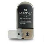
wide 1

ICCAD at 30: Alberto Looks Back and Forward

ICCAD at 30: Alberto Looks Back and Forward
by Paul McLellan on 11-08-2012 at 8:10 pm

At ICCAD earlier this week, CEDA sponsored a talk by Alberto Sangiovanni-Vincentelli looking back over the last 30 years (it is the 30th anniversary of ICCAD) and looking to the future. As is always the case in these sorts of presentations, the retrospective contained a lot more detail than the going forward part. Clayton Christensen had an editorial in the New York Times just the weekend before looking at the different types of innovation. And, by the way, if you have never read Christensen’s The Innovator’s Dilemma then you absolutely should.


Christensen identifies three types of innovation and Alberto picked up on these in the context of EDA. First is empowering innovation. This transforms complicated products available only to a few into simpler products available to many. For example, the Ford Model T or Sony’s first transistor radio. This type of innovation creates jobs since more people are required to create and sell the new products. They also use capital to expand capacity.

Next is sustaining innovations. These replace old products with new models. But they replace them. Hybrid cars such as my Camry replace non-hybrid cars. It’s not as if I kept my old car too, never mind bought a second new one. In terms of dollars this is probably the biggest part of innovation but it has a neutral effect on economic activity and capital. It’s more of a zero-sum game.

Then there are efficiency innovations. These reduce the cost and disrupt existing products: steel minimills, or the PC for example. They streamline processes and actually reduce employment and often (but not always) require less capital.


Alberto reviewed EDA as going through phases. In 2005, if you looket at the most cited papers in computer science–all of it, not just EDA–then the top 3 were all in EDA. The best minds in algorithms were working in EDA (if you are intereseted, the top 3 were Kirkpatrick et al’s paper on simulated annealing, Randy Bryant’s paper on BDDs and Harel’s paper on state-charts).

Today, EDA is more of a mature industry. While there is some innovation going on, of course, a lot is more like the efficiency innovation, making the algorithms that we already have work on larger designs.

One thing Alberto pointed out is that we have an incredible body of smart engineers working in EDA. We understand how to handle unimaginably complex data with incredibly efficient algorithms. We know how to abstract, simplify and generally manage enormous complexity. For example, if you look at the state of the art in mechanical CAD it is primitive compared to what is required to design an IC. Alberto reckons that if EDA is going to grow then we have to re-define EDA to include more stuff and then we can deploy our engineering skills more widely. One place that EDA missed was a lot of the system design stuff. Although they are private so nobody knows the exact numbers, The Mathworks’ Matlab and Simulink are a billion dollar business, in a space just adjacent to EDA.


IJTAG, Testing Large SoCs

IJTAG, Testing Large SoCs
by Paul McLellan on 11-08-2012 at 5:57 pm

Test is the Rodney Dangerfield of EDA, it doesn’t get any respect. All designs need to be tested but somehow synthesis, routing, analog layout and the rest are the sexy areas. In my spoof all purpose EDA keynote address I even dissed it:You are short on time so slip in a quick mention of manufacturing test. Who knows anything about it? But chips have to be tested so talk about scan. Or BIST. Or ScanBIST.

It is about a $120M business with Mentor being a little over half of it. But test is getting more important driven by two things. Firstly, chips are huge and consist of many IP blocks that were not designed and are barely understood by the SoC design team. Another big driver is 3D ICs (probably even more in the future). Testing a stack of die when only the lowest one is accessible to the tester creates its own set of challenges. But what is called the “known good die” problem is another driver. In a conventional (non 3D) IC, if a bad die makes it through to final test then a package needs to be discarded along with a die that was bad in any case. But in a 3D IC stack, if a bad die makes it all the way to final test, not only is the package and a bad die discarded, but several good die too. So wafer sort for 3D IC is much more important than before.


Mentor has just announced an IJTAG solution that addresses both these drivers, that chips increasingly consist of IP blocks which the designers do not fully understand and that 3D just adds another layer of complexity. It supports the catchily-named IEEE P1687 standard (IJTAG) and allows designers to easily reuse test, monitoring and debugging logic embedded in the IP blocks. It generates an integrated hierarchical contro9l and data network with a single top-level interface for the whole SoC. Any embedded instrumentation that is P1687 compliant can be used. It is especially valuable where pin count is limited or access is difficult (as in the 3D stacked die configurations).

The new IEEE P1687 standard creates an environment for plug-and-play integration of IP instrumentation, including control of boundary scan, built-in self-test (BIST), internal scan chains, and debug and monitoring features in IP blocks. The standard defines hardware rules related to instrumentation interfaces and connectivity between these interfaces, a language to describe these interfaces and connectivity, and a language to define operations to be applied to individual IP blocks. IJTAG replaces proprietary and incompatible IP interfaces from multiple suppliers with a standardized interface mechanism that enables plug-and-play integration of IP test and instrumentation facilities.

Mentor’s Tessent IJTAG solution provides automated support for the IJTAG standard, substantially reducing the time and effort required to assemble large SoC designs from reusable IP blocks. The new product includes all the facilities needed to efficiently integrate IEEE P1687-compliant IP into a design:

  • Automatic verification that a given IP block is compliant to the P1687 standard
  • Verification that P1687-compliant IP blocks are properly connected within a P1687-compliant access network
  • Automatic creation of a P1687-compliant access network connecting IP to the top level instrument interface
  • Retargeting and merging of local IP instrumentation patterns through the P1687 network, allowing IP specific sequences to be applied from chip pins or from anywhere higher up in the system hierarchy

The white paper on Tessent IJTAG is here.


ARM adopting SpyGlass IP Kit, joining TSMC’s soft IP9000 Quality Assessment Program

ARM adopting SpyGlass IP Kit, joining TSMC’s soft IP9000 Quality Assessment Program
by Eric Esteve on 11-07-2012 at 12:17 pm

More than one year old now, TSMC’s soft IP quality assessment program is a joint effort between TSMC and Atrenta to deploy a series of SpyGlass checks that create detailed reports of the completeness and robustness of soft IP. This soft IP quality program has been the first to be initiated by a Silicon foundry on other than “Hard IP”, and is demonstrating how IP support, whether hard or soft, is important in TSMC strategy to best support their customers and shorten the design to Silicon delay and reduce the TTM. Currently, over 15 soft IP suppliers have been qualified through the program, including ARM, as recently announced by TSMC at ARM TechCon.

How does the flow works? Atrenta’s SpyGlass® platform provides a powerful combination of proven design analysis tools with broad applicability throughout the SoC flow. The SpyGlass platform includes a tool suite for linting, CDC verification, DFT, constraints analysis, routing congestion analysis and power management applicable at RTL as well as the gate level. Providing visibility to design risks early and at high design abstractions, SpyGlass enables Early Design Closure® –During the course of chip development, design goals evolve and get refined from the initial RTL development phase to the final SoC implementation phase. The SpyGlass platform offers a consistent solution that can be used effectively at each stage of the design process to achieve the respective design goals. The use of the right SpyGlass tools at the right stage of design development helps design teams achieve a predictable repeatable methodology.

The list of design goals addressed by GuideWare, a set of pre-packaged methodologies for SpyGlass, show that the risk of failure is early addressed, and can be minimized:

  • Will the design simulate correctly?
  • Are clocks and resets defined correctly?
  • Will the design synthesize correctly? Are there unintended latches or combo loops?
  • Will gate simulations match RTL simulations?
  • What will the test coverage be?
  • What is the power consumption of a given block?
  • What is the profile of this IP? (For example, gates, flops, latches, RAMS/ROMS, I/Os, tristates, clocks)
  • Are there any inherent risks or non-standard design practices used in this IP?
  • Are there any adaptation issues in the target SoC, such as power, routability or congestion?
  • Are all the incoming blocks truly ready for integration? Are they clean in terms of clocks/resets and constraints?
  • What are possible inter-block issues? (For example, are block-level constraints complete and coherent with target SoC constraints?)
  • What are “common-plane” issues among heterogeneous blocks? (For example, scan chain management and test blockages at the SoC level)
  • Can I leverage my block-level work (waivers, constraints) at the SoC level?

Coming back to TSMC soft IP quality assessment program, we can see that the list of IP partners is a who’s who including from Network-on-Chip IP vendor Arteris, DSP IP core supplier CEVA, PCI Express IP core (PLDA), configurable CPU IP core (Tensilica) to GPU and CPU IP core vendors with ARM Ltd. and Imagination Technologies, Video and Display IP (Chips and Media), and scanning also Dolphin Integration, Cosmic Circuits or GlobalUniChip, provider of mixed-signal IP. That’s really make sense that ARM, the #1 IP vendor, join this program, as well as it would really makes sense that at least two of the top 3 EDA & IP vendor, Cadence and Synopsys, would join the program, sooner or later…

Eric Esteve from IPNEST


Solido and TSMC for 6-Sigma Memory Design

Solido and TSMC for 6-Sigma Memory Design
by Daniel Nenni on 11-06-2012 at 8:30 pm

Solido Design Automation and TSMC recently published an article in EE Times describing how Solido’s High-Sigma Monte Carlo tool is used with TSMC PDK’s to achieve high-yield, high-performance memory design. This project has been a big part of my life for the past three years and it is time for a victory lap!

In TSMC 28nm, 20nm and smaller process nodes, achieving target yields is extremely challenging. Nowhere is this truer than for memory circuits, which aggressively adopt next bleeding-edge process nodes to help meet increasingly tighter performance specifications and higher levels of integration.

The article reviews the challenges raised by process variation, and in particular for memory with its high-sigma components. The article then discusses an approach to address variation with accurate statistical MOS modeling, plus the ability to analyze billions of Monte Carlo samples in minutes. This solution is now in place and rapidly gaining adoption.

The core reason for poor yield in memory is due to advanced process variations. The chips that roll out of manufacturing do not perform to the ideal, nominal simulated versions in design. If they do not meet parametric yield, they can’t be used. Process variation comes in many forms such as random dopant fluctuations, variations in gate oxide thickness, line edge and roughness. But their effect is the same: these random physical variations translate to variations in electrical device performances such as threshold voltage and transconductance. In turn, the device performance variations translate to variations in circuit performance such as power consumption, read current in a bitcell, or voltage offset in a sense amp. In turn, circuit performance variation means chip performance variation, causing yield loss.

The reason that variation is such an issue at 28nm and below is that the device sizes are getting within the same order of magnitude as the size of atoms themselves. We used to have Avogadro-size counts for the number of atoms in a device; but now those counts are in the thousands. The oxide layer on gates is down to just a few atoms thick, so even one or a few atoms out of place can cause performance variation of 20% to 50% or more.

The first case study in the article is a 6 transistor bitcell, using statistical device models from the TSMC 28nm PDK. With 6 devices, it has 60 local process variables. The second case in the article is a sense amp delay, having 15 devices and 150 process variables, also using statistical device models from the TSMC 28nm PDK.See the full articleHERE.

Also see:

EDA Tools to Optimize Memory Design, Size Standard Cells, Verify Low-Power Design, Center Analog Designs

TSMC Theater Presentation: Solido Design Automation!

Solido Design Automation Update 2012


High Yield and Performance – How to Assure?


A Survey of High-Sigma Monte Carlo Analysis Approaches


High-efficiency PVT and Monte Carlo analysis in the TSMC AMS Reference Flow for optimal yield in memory, analog and digital design!


Solido & TSMC Variation Webinar for Optimal Yield in Memory, Analog, Custom Digital Design


PVT and Statistical Design in Nanometer Process Geometries


Semiconductor Yield @ 28nm HKMG!


Solido – Variation Analysis and Design Software for Custom ICs


Variation Analysis


Variation-aware Design Survey


Moore’s Law and 28nm Yield


Embedding 100K probes in FPGA-based prototypes

Embedding 100K probes in FPGA-based prototypes
by Don Dingee on 11-06-2012 at 8:15 pm

As RTL designs in FPGA-based ASIC prototypes get bigger and bigger, the visibility into what is happening inside the IP is dropping at a frightening rate. Where designers once had several hundred observation probes per million gates, those same several hundred probes – or fewer if deeper signal captures are needed – are now spread across 10M gates or more.

That sparseness causes choices, and if through divine inspiration probes are placed where the problem is, there is some debug visibility to help solve issues. Most engineers aren’t that fortunate, especially with unfamiliar third party IP, and debugging is trial-and-more-error. While probes can be moved around in an FPGA-based prototype until the problem is isolated, re-synthesis is a process that takes hours, usually reserved for overnight runs.

Daniel Payne gives us an introduction to Brad Quinton, creator of the technology inside the Tektronix Certus 2.0 FPGA-based prototyping debug solution. I’d first heard about Brad’s approach in 2010, prior to his company Veridae Systems being acquired by Tektronix. He used the following chart from ITRS to illustrate the problem:

While the escape rate of bugs per 100K lines of code (LOCs) improves, it is outstripped by the growth in RTL LOCs for bigger designs, and the result is an out-of-control increase in escapes. The issue Brad has been after is how to add more probes to an RTL design without chewing up major resources in an FPGA.

There are several key technologies in play in Certus:

Efficient embedded instrumentation: A small block of RTL comprising a probe can be placed on just about anything in the FPGA, connected to an infrastructure with a multi-stage concentrator using fewer LUTs than traditional probes in FPGAs. These placements are done automatically using the Implementor tool in any FPGA EDA flow, and it allows control over how many LUTs are allocated to the debug infrastructure. Using OptiRank, design RTL is analyzed, and signals are ranked producing recommendations for the best coverage.

Longer debug traces: Traditional FPGA probing can capture limited amounts of data, usually a few seconds, at-speed. However, to see problems develop, often more than a few seconds of data is needed, a difficult task for on-chip resources with limited RAM. External analyzers can be used but they have to be synchronized carefully. In Certus, capture data from each probe is compressed in a lossless algorithm which takes advantage of repeated patterns common in traces, resulting in extended trace depths. These figures aren’t typical but represent what is possible in trace depths:

Time-correlation analysis:Certus collects time-correlated data system wide from all the probes at full speed of the FPGA-prototyping system, and presents it on a single JTAG interface. Using the Analyzer tool, designers can zoom in and create complex triggers on the data of interest. Instead of re-instrumenting and re-synthesizing the FPGA, designers can just run scenarios and go to the data. Another benefit of this is unique to FPGA-based prototyping systems: since the data collected from multiple FPGAs is time-correlated, partitioning problems and issues with multiple clock domains can be identified quickly and easily.

In significantly less time than it would take a designer to place 1K probes using traditional tools, up to 100K probes can be placed using Certus. Once that placement is synthesized in, designers can concentrate on running scenarios and analyzing and fixing design RTL instead of recompiling instrumentation just to identify the issues.

The Tektronix approach in Certus brings instrumentation to any FPGA-based prototyping system, creating the opportunity for much deeper visibility similar to an RTL simulator or emulator, but with much faster speeds of operation. See the Tektronix White Papers Wiki for a white paper describing bottlenecks Certus addresses, and a case study from the Dini Group on Certus use.


A Most Significant Man

A Most Significant Man
by Beth Martin on 11-06-2012 at 8:10 pm

Most of us live perfectly good lives without distinction, fame, or note. Others rack up the honors, filling their walls and resumes with recognition of their brilliance. Like Dr. Janusz Rajski.

Rajski is the director of engineering for the test products at Mentor Graphics, an IEEE Fellow, and the inventor of embedded deterministic test technology that is the core of Mentor’s TestKompress product. He has collected a whole stable of best paper awards, and today he picked up another at the ITC (International Test Conference). The Most Significant Paper award recognizes a paper from 10 years ago that has had lasting impact and significance.

Rajski was the lead author on “Embedded Deterministic Test for Low-Cost Manufacturing test,” published at ITC in 2002. The paper introduced embedded deterministic test technology (EDT), which was a breakthrough technology and is now absolutely indispensable to the testing of today’s ICs. The paper was highly significant at the time of publication and had a big impact on further research and technology. Not only that, but it is still relevant to R&D and industrial practice.

I mentioned that Rajski is impressive, right? Here’s what I mean: 69 U.S. patents (and 70 more pending) in the field of logic synthesis and silicon test, IEEE Donald O. Pederson Award, eleven IEEE best Paper Awards or honorable mentions (not counting the Most Significant ITC paper award), Stephen Swerling Innovation Award, 200 IEEE technical publications, 65 papers in other scientific journals, and 135 papers in conference proceedings. Just listing all that made me tired. But Rajski, he’s still at the top of his game.


Should ARM care about MIPS acquisition?

Should ARM care about MIPS acquisition?
by Eric Esteve on 11-06-2012 at 3:09 am

It was not really a surprise to learn that, finally, MIPS have been sold, as the company was officially for sale since April 2012. Nevertheless, the interesting part of this news comes from the buyer’ identity: Imagination Technologies. Imagination is an UK based company, like ARM, selling processor IP cores, like ARM, but the (huge) difference was coming from their port-folio: Imagination only sales Graphic Processing Unit (GPU) IP cores, when ARM sell both CPU (the Cortex family) and GPU (MALI family), as well as Libraries and some Interface IP like DDRn Controller. Should we mention that ARM CPU IP cores are ultra-dominant in the mobile application like smartphone, media tablet, and any kind of wireless phone? I have heard about ONE design-in of MIPS CPU IP in this mobile multi segments, one out of hundreds. On the other hand, Imagination has seen a very good penetration of the PowerVR family of GPU in these mobile segments, even if MALI GPU IP had significantly increase penetration in 2011, but not at the level of PowerVR GPU IP.

In summary, in the mobile segments, you need two essential pieces, the CPU and the GPU IP cores, to build and Application Processor, as well as several dozens of other IP functions, but that’s not the topic of today. ARM is ultra-dominant with the Cortex CPU IP family (A9, A15 and now the big-little A57-A53 dual cores), when Imagination Technologies is dominant (but not “Ultra”) with the PowerVR GPU IP family, both addressing various market segments and application (smartphone, media tablet, set-top-box, HDTV… to name a few), the most lucrative being, by far, the mobile segment, with smartphone shipments forecast being in the range of 680 million units for 2012 and media tablet in the range of “only” 100 million (plus) units for 2012.

When ARM is attacking Imagination Technologies best seller product GPU IP core, with MALI family increasing penetration, that’s a threat for Imagination. But when Imagination Technologies buying MIPS and the related CPU IP cores product line, is it really a threat for ARM? If we look at the customer installed base, especially in the mobile market, we don’t expect the Qualcomm, Apple, Samsung and others to move to MIPS CPU in the short or even mid term. They could use MIPS in the license or royalties price negotiation with ARM, but changing architecture would be a highly risk bid… and what could be the benefit? Saving a few, or even a dozen million dollar is not a good enough reason to put such profitable product lines at risk, for these already installed and making good money in the mobile segments.

But, for the numerous new comers, most of them being based in China and attacking the largest mobile market (in units) worldwide, if ARM CPU IP core is certainly the most attractive solution, the cost of ownership could be a good enough reason to move –or to start- with MIPS core. As soon as their installed product base, and the related million lines of S/W developed, is not too large, they could decide to take a chance and select MIPS… Imagination will be able to address both the CPU and GPU IP cores needs, and grab some market share in various segments, nevertheless, considering how wise the company development was so far, ARM will certainly build the proper strategy to address this new deal, like they did in the past when fighting with MIPS. If you’re not convinced, just look at where MIPS has fallen today!

From Eric Esteve– IPNEST


Waiting or EUV – Another View on the ReRAM Roadmap

Waiting or EUV – Another View on the ReRAM Roadmap
by Ed McKernan on 11-05-2012 at 9:03 pm

It is ‘Quarterly’ financial report time for many companies and one can occasionally find some interesting snippets in the transcripts of the calls which normally accompany these announcements. For example, SanDisk appear to have an encouraging quarter, reversing sales declines seen through Q1 and Q2. However, what caught my eye was this quote attributed to SanDisk’s CEO Sanjay Mehrotra “We also believe that 3D ReRAM will not start production until sometime beyond 2015 given its need for EUV lithography, which is still in development phase.” (A similar comment is buried in the presentation made by SanDisk at their Analyst’s day in February this year.) This is somewhat more conservative than other company’s roadmaps as we have discussed at ReRAM-Forum.com. Coincidentally the annual EUV Lithography Workshop has just been held in Hawaii in June and the more recently, the EUV Source Workshop held in Dublin in October. Both the EUV Workshops have full proceedings on-line at www.euvlitho.com. In a bit of a departure from our regular Blog focus, we have taken a look at EUV as it appears to be a key factor in the ReRAM roadmap of at least one major memory company. For more information go over to www.ReRAM-Forum.com.


Gustafson on Parallel Algorithms

Gustafson on Parallel Algorithms
by Paul McLellan on 11-05-2012 at 4:54 pm

At the keynote for ICCAD this morning, John Gustafson of AMD (where he is Chief Graphics Product Architect as well as a Fellow) talked about parallel algorithms. Like Gene Amdahl, whose law states that parallel algorithms are limited by the part that cannot be parallelized (if 10% is serial, then even if the other part takes place in zero time, the maximum speedup is 10X), Gustafson has a law named after him. It basically says Amdahl is wrong, that there is no limit to the speedup you can get as long as you increase the size of the problem along with the number of cores. So his talk was a look at whether there are embarrassingly serial problems, problems that are not open to being parallelized.

For example, at first glance, calculating the Fibonacci series look like one. Each term depends on the previous two so how can you bring a millions servers to bear on the problem. But, as anyone who has done any advanced math knows, there is a formula (curiously involving the golden ratio) so it is straightforward to calculate as many terms as desired in parallel.


By 2018 we should have million server systems each doing teraflops through highly parallel operations running on GPUs. The big challenge is the memory wall. For operations that involve a high ratio of work to decision making, this sort of SIMD (single instruction, multiple data) can significantly reduce wattage per teraflop.


Throwaway line of the day: with great power comes great responsibility…and some really big heatsinks!

An instruction issue consumes around 30 times more power than basic mutiply-add operations and a memory access much more power than that. Memory transfers will soon be half the power consumed and processors are already power-constrained. Part of the problem is that hardware caches are very wasteful, designed to make programming easy rather than keep power down. They minimize miss-rates at the cost of low utilization (around 20%). Even more surprisingly, only 20% of the data written back out of the cache is ever accessed again so didn’t really need to be written back at all. John felt that at least for low-level programmers we need a programming environment that makes memory placement visible and explicit (as it apparently was on the Cray-2).


There are two ways to associate a SIMD GPU with a processor: on-chip and a separate off-chip device. On chip seems to work best for problems where data re-use is 10-100 (such as FFT and sparse-matrix operations) and an off-chip device works best for data re-use in the 1000s, such as dense matrix and many body dynamics.

We also need better arithmetic. Most programmers have never studied numerical analysis and so have no idea how many bits of precision there are or how to calculate it. A specific problem is that accumulating results (by adding) needs much more precision that is used to calculate the numbers to add. Eventually you are adding small numbers to a number that is so large that it doesn’t change. John had a few examples where he was using 8 bit floating point (yes, really. 1 sign bit, 3 bits of exponent and 4 bits of mantissa) but doing accurate analysis.


John’s final conclusion: if we really cherish every bit moved to and from main RAM then we can get better arithmetic answers (provable bounds) and as a side-effect help the memory wall dilemma and always have a use for massive parallelism.