Everyone understands that as we increasingly focus on the design of mobile devices, there is an increasing focus on low power. But, what is implied in designing for low-power? Designing for low power means we have to work with multiple power domains and multiple clock domains—making our design task more complex. We also must get these new mobile devices to market quickly, causing shorter design cycles. To accomplish this, more reusable IP blocks are typically utilized because they introduce fewer errors since these IP blocks are pre-verified. However, more IP blocks and more subsystems also bring more power domains in order to maximize the battery life of the end products.
[The diagram above shows the results of an industry survey regarding on-chip communications networks taken in October 2012 and commissioned by Sonics, Inc.]
With the increasing number of power and clock domains, there is a connection complexity which is growing exponentially. We need to connect all the different pieces of the design. This is difficult not just due the large number of functional blocks, but also the many unique combinations of power and clock domains. We are now hearing of designs with more than 20 power domains and more than 50 clock domains. Whereas, a set-top box ten years ago may have included a memory bus, peripheral bus, and some specialized buses for pipeline operations, these new designs must include a huge number of different connections.
To meet our design goals, we need to try for an optimal grouping of blocks as well as optimize the use of different connection styles. The connection styles include various standard interface protocols (e.g., OCP, AXI, or AHB), along with fabric choices such as routers, switches, and crossbar implementations. Managing the large numbers of connections of various types in a modern mobile design clearly creates a complex on-chip communications network (OCCN) design problem.
The primary goals in designing an on-chip network architecture for a chip in a mobile product now include:
(1) Meeting the performance goals of the design—frequency and latency;
(2) Optimizing grouping and choice of connection-type for the various domains; and
(3) Keeping the interconnect within the allowable wire congestion and area tolerances—by reducing the overall design effort using automation.
In selecting an on-chip network partner, consideration needs to be given to ensure that the vendor supports multiple fabric connection styles and a strong environment to analyze the network design choices that are made. This means looking beyond just the type of connection. For example, in some cases the designer can trade-off between ‘serializing’ versus ‘parallelization’ of the data—meaning wider or deeper channels. Of course, the design must consider many other complex trade-offs such as the number and use of virtual channels (a single physical connection that can have many logical connections).
The vendor that provides all this is Sonics, Inc. Sonics’ StudioXE™ development environment contains both graphical and command line tools to aid the user in the design process from architectural exploration to synthesis. The environment automates several design phases—saving the designer time by automating the creation of synthesis scripts, design constraints, timing analysis input preparation, and design-for-test management.
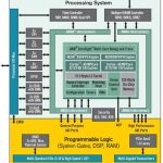
To help you meet your performance goals, Sonics has several on-chip networks available as design IP. Among these networks is SonicsGN™ (SGN), Sonics’ fourth-generation configurable on-chip network that includes native socket interfaces like AXI and OCP and uses a router-based fabric or ‘NoC’ (network-on-chip). SonicsGN enables the user to design advanced SoC communications networks by using a high-speed scalable fabric topology structure and is also the industry’s highest frequency NoC available today. The SGN architecture is particularly well suited for low-power designs by allowing for virtually an unlimited number of power, clock and voltage domains. The design tools provide the automation for these domains to be partitioned anywhere in the network, simplifying the SoC design task. In addition, SGN provides the signaling interface at each domain to allow a power manager unit to rapidly and reliably turn domains on and off. This level of control will save significant power over the traditional method of relying on software and the CPU.
For modern low-power design of mobile devices SGN is the type of network IP fabric that designers will need. Coupled with the other configurable connection in the portfolio, plus their StudioXE development environment, Sonics should be at the top of any designers list when it comes to solving mobile product design challenges.