One of the challenges in doing a complex analog or mixed signal design is that things get out of step. One designer is tweaking the schematic and re-simulating, another is tweaking the layout of transistors, another is changing the routing. This is not because the design flow is messed up, but rather it reflects reality. If you wait until the schematic is finished to start layout, then you won’t finish in time. And besides, in a modern process, without detailed layout parasitics you can’t simulate the design accurately and so have the information needed to finish off the schematic. You need to make smaller and smaller changes and cross your fingers that everything converges on a layout that will give you the performance you require.
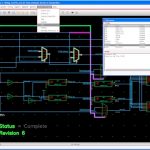
But this means that the schematic that goes with the current layout is not necessarily the most up-to-date. What is needed is a tool for comparing schematics and layouts. Obviously, these are stored in text or binary files which generally are not human readable and so a traditional diff program that simply tells you what changed in the file is useless. What is required is a visual diff that displays differences graphically, showing added transistors on the schematic or layout that has been moved. ClioSoft’s vdd (Visual Display Diff) is just such a tool.
VDD detects changes between different versions of schematics or layout including modifications to nets, instances, layers, labels and properties. Differences are highlighted graphically in the Cadence Virtuoso schematic or layout and also presented in a list. Users can select or step through the list. Selected changes are highlighted directly in the editor window and automatically zoomed to the area of interest. VDD has the option to ignore cosmetic changes so mere rearrangement or rerouting of wires will not be flagged. Users also can choose to invoke a hierarchical diff where all differences for the entire design hierarchy below the selected view will be flagged. VDD comes integrated with ClioSoft’s SOS design data management system but also can be deployed standalone with any other design management system or even if no design management system is being used.
ClioSoft have a game here called Spot the Diff where you have to find differences in schematics. Of course it is just a bit of fun but it has a serious purpose: finding changes by eye is really hard and time-consuming. That is why a tool like VDD is so essential.
Leading semiconductor companies including many in the top 10 are using VDD. You can find out more in an upcoming webinar presented by Srinath Anantharaman of ClioSoft, Managing Design Reviews and ECOs Efficiently. It is on Thursday September 12th at 11am Pacific. Details are here. Registration page is here.
Also Read