You are currently viewing SemiWiki as a guest which gives you limited access to the site. To view blog comments and experience other SemiWiki features you must be a registered member. Registration is fast, simple, and absolutely free so please, join our community today!
As I have mentioned 28 times already, on Friday (April 19[SUP]th[/SUP]) I will be keynoting FinFET day at the EDPS conference in Monterey. This is an excellent opportunity to ask the experts about the challenges of FinFET design and manufacturing in an intimate setting (60 people). If you are interested register today and use the promo codeSemiWiki-EDPS-JFR and save $50.
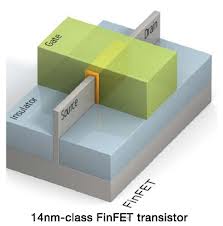
I wrote about the morning session here: FinFETs: Ask the Experts!I just reviewed the final slides and WOW! The presentations from Raymond Leong and Tom Dillinger are the best FinFET content slides I have seen yet! Don’t miss this event! Seriously, WOW!
In the afternoon there will be a panel discussion with Betty Pokerwinskiof Qualcomm, John Heinleinof Arm,Luigi Capodieciand Srinivasa Bannaof GLOBALFOUNDRIES. I will be moderating and I would like to thank everyone that helped with the questions. They are still coming in but this is what I have so far:
[LIST=1]
What can we do to improve early engagements with customers?
What challenges your team the most going from a previous process node to FinFET?
Which IPs libraries will have the highest impacted going to FinFET?
Can you expand on IOs, ESD structures, and analog components (diodes, resistors, capacitors)?
What are the trade-offs for the standard cell track heights between planar and FinFET?
How is FinFET technology giving you more opportunity to broaden your market, low power to server core performance? (ARM)
How are you working with the foundries to reduce VDD_min for very low power applications?
Is ARM adding to core designs additional error detection and recovery circuits for FinFETs?
What does GF see as trade-offs for FinFET fabrication for bulk versus SOI?
How does GF develop a process to address the range from very low power to high performance server and communications market?
What do you see for FinFET layout dependent effects compared to planar?
Do you see any new or more severe reliability failure mechanisms or transistor drift with FinFETs?
FinFET offers higher drive current and higher gate capacitance. So is there a netbenefit in performance at Iso Power or reduction in power at Iso frequency?
Do FinFETs bring any benefits to SoC area scaling? Is so what are some thoughts on area scaling?
What else can we do in EDA for you in regards to FinFET Parasitic extraction, Electro migration (EM), Thermal Modeling?
What other challenges are you experiencing that may not have been touched on here?
I need four more so we can play 20 questions.Post them in the comment section or email them to me directly.The panel starts right after lunch and alcohol will be served so expect the unexpected!


 As I have mentioned 28 times already, on Friday (April 19[SUP]th[/SUP]) I will be keynoting FinFET day at the EDPS conference in Monterey. This is an excellent opportunity to ask the experts about the challenges of FinFET design and manufacturing in an intimate setting (60 people). If you are interested register today and use the promo codeSemiWiki-EDPS-JFR and save $50.


TSMC CoWoS versus Intel EMIB Semiconductor Packaging