How to best forecast a specific protocol adoption? One option is to look at the various IP sales, it will give you a good idea of the number of SoC or IC offering this feature on the market in the next 12 months. Once again, if you wait for the IP sale to have reached a maximum, it will be too late, so you have to monitor the IP sales dynamic when the sale volume is still in the low range to make an efficient analysis, which can help you taking the right decision just a little bit in advance in respect with your competitor – to benefit from a Time-To-Market advantage. That’s why we will mention the clear winners, demonstrating high market penetration (and becoming “de facto” standard in certain market segments), and also put the focus on the emerging protocols demonstrating fast growing penetration.
The above table is extracted from the “Interface IP Survey” version 5, just completed. In short you will discover in this survey:
- IP vendor ranking, protocol by protocol, by IP License revenue, for USB, PCI Express, HDMI, SATA, MIPI, DisplayPort, Ethernet and DDRn Memory Controller,
- Competitive analysis by protocol
- Controller and PHY IP license price (by technology node for PHY)
- By protocol adoption rate and market trends
In fact, IPnest is the only analyst proposing such a granularity and this approach has allowed building a large customer base, including IP vendors, ASIC Design House, Foundries, Fabless and IDM. Ranking of the numerous IP vendors by protocol is very useful, but not enough, IPNEST has inserted market intelligence and not only raw data!
The winners in 2013
HDMI is again this year a very successful protocol, both in term of market penetration in the Consumer/HDTV segment and in term of pervasion in various segments like PC, Wireless Handset (smartphone), Set-Top-Box, DVD players and recorders, Digital Camcorder, Digital still camera and even Automotive (I guess thanks to platforms like TI OMAP, as the chip maker has to enter in new segments after giving up in the wireless). Analyst consensus is that almost 3 billion HDMI ports have been shipped since the protocol inception. DisplayPort has become complementary to HDMI, the adoption has been confirmed in 2012, after a strong growth in 2011: the protocol is well tailored for interfacing a PC and a screen, that’s naturally here that the adoption is high. We clearly rank DisplayPort in the winner list.
According with Silicon Image, the adoption for “Mobile High-Definition Link” (MHL) is growing very fast. MHL provides the same bandwidth capability (and compatibility) that HDMI 1.4… but with a micro-USB (5 pin) connector instead of the traditional HDMI connector. Just keep in mind that MHL will be primarily used in mobile electronic systems, smartphones, media tablet and probably notebook and ultrabook PC. That makes over one BILLION potential devices integrating MHL in 2013…
The semiconductor and electronic industry had in the past some concerns with HDMI protocol: they had to pay royalties to HDMI LLC, but they could not influence the specifications. Until late 2011, HDMI LLC was a closed standard body that consisted in seven founders and over 1,000 adopters. The HDMI specification was architecture by the seven founders in a closed-door environment. In October 2011, the HDMI founders established a nonprofit corporation called HDMI Forum, with the purpose to foster broad industry participation in the development of future versions of the HDMI specification.
Efficient basic protocol, plus two new releases, one addressing the form factor of the connector (MHL) and the second extending HDMI to more HD with 2.0, sold to customers happier today than in the past, that makes good reasons for HDMI IP sales to jump in 2012 and growing again in 2013.
MIPI is a set of interface specifications initially specifically tailored for wireless phones system, defining almost any kind of chip to chip interface: Camera to Application Processor (AP) with CSI, Display with AP (DSI), Baseband with AP (Low Latency Interface, allowing to share an external DRAM), main SoC with RF chipset (DigRF) and another dozen specifications. I will come back to MIPI in a next blog very soon, explaining why MIPI IP sales have been multiplied by x4 from 2010 to 2012, seeing a 60% increase in 2012.
To give a complete picture about MIPI, it’s important to notice that the MIPI Alliance has consolidated MIPI positioning within the Interface Ecosystem, by concluding very promising agreements with three standard organizations:
- JEDEC: definition of Universal Flash Storage (UFS), to be used in conjunction with MIPI M-PHY, offering within a mobile system
- USB-IF: specification of SuperSpeed USB Inter Chip (SSIC), where the USB 3.0 PHY can be replaced by MIPI M-PHY, offering high bandwidth and low power capabilities for chip to chip communication in a mobile system
- PCI-SIG: definition of “Mobile Express”, delivering an adaptation of the PCI Express® (PCIe®) architecture to operate over the MIPI M-PHY® physical layer technology
We will use these agreements to introduce the next two Interface protocol winners: USB 3.0 and PCI Express.
SuperSpeed USB IP have started selling well during 2012, with a design start count being last year equal to the sum of design starts during 2009, 2010 and 2011. In the meantime, many IP vendors have given up (PLDA, Snowbush to name a few), and the result is that there is a clear, undisputed winner in the USB 3.0 market: Synopsys! But Cadence has made two acquisitions during 2013, Cosmic Circuit and Evatronix, the first bringing USB 3.0 PHY IP and the second USB 2.0 integrated solution plus USB 3.0 Controller IP, indicating that the EDA & IP vendor did not give up about MIPI. Fair competition is always good for the market! Moreover, USB-IF is launching USB 3.1, offering a (doubled) 10 Gbps data rate. Offering a solid roadmap is always a good indication that a protocol will live for a long time; it could also be a good way to change the deal, or the IP vendor landscape.
PCI Express penetration has started in 2005 and has never stopped since then. The technology has been adopted in many, many market segments, with the notable exception of Consumer Electronic and mobile wireless. In fact PCIe success will go even further, as at the end of 2011, SATA-IO Organization has decided to offer ‘SATA Express”, the Non Volatile Memory storage application interface will be supported by NVM Express and in 2012 MIPI Alliance has defined “Mobile Express”.
If we take a look at PCI Express IP cumulated revenues since its inception, we realize that the technology has generated more than $300M of license IP business. We can mention four reasons why PCIe IP sales should continue to grow:
- PCIe gen-3 (8 Gbps) is selling well, at higher price than gen-2
- PCIe gen-4 (16 Gbps) is probably in the pipe to be finalized in early 2015, expect fewer IP sales than gen-3, BUT at much higher pricing (PHY IP over $1M)
- Mobile Express IP sales are net growth, the standard is new
- SATA Express as well, NVMe is more questionable
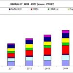
This last protocol is seeing a wide adoption, or more precisely a growing outsourcing rate and simply the faster growing and larger IP sales: DDRn. DDRn controller is a mean to interconnect a SoC with memory, using a digital part (Controller) and a physical media access (PHY), so it’s built like every other modern high speed protocol. We have shown in the “Interface IP Survey” that, even if the ASIC design starts decline year after year, the SoC proportion of these design start is growing higher. Because there is more SoC design starts, a SoC being defined as a chip integrating one or more processor (CPU, GPU, DSP, and Microcontroller), the net number of DDRn controller is growing at the same rate. Because the DDRn controller design from scratch is becoming more difficult to manage with DRAM frequency increase, leading to move from ‘Soft PHY” to hardened PHY for example, the move to external sourcing of DDRn controller IP is growing faster than any other Interface IP. This looks theory, but we can see effective sales of DDRn controller IP growing on line with the thory! Just look at these results from IPNEST for 2008-2012. DDRn IP segment is strongly growing, and the leadership is split between Synopsys (again), Cadence (thanks to Denali acquisition) and ARM.
Misc… but not least: Network-onChip
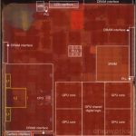
Network on Chip (NoC) is not a protocol, neither an interface, rather an interconnect function, buried into a SoC, to connect, manage and monitor the multiple IP blocks. As such a NoC will be, by definition, connected to all the interface functions, from DDRn memory controller to USB, PCIe, UFS and so on. That we have seen in 2011-2013 is the strong penetration of NoC IP into various market segments (Wireless, Consumer Electronics, Automotive and more), although the NoC was at concept stage in the mid-2000. This trend has been so effective that a NoC IP vendor like Arteris has incredibly increase revenue coming from upfront licenses between 2010 and 2012. But trees don’t grow up to sky, everybody knows this… Qualcomm buy it before, like the company did with Arteris for a (supposedly) amount of a quarter billion dollar. Semiwiki told you last year how good was Arteris, thanks to Qualcomm to confirm our views.
The losers in 2013
Just take a look at the same article written last year, as there is no new comer in this list!
Eric Esteve from IPNEST –
Table of Content for “Interface IP Survey 2008-2012 – Forecast 2013-2017” available here.
More Articles by Eric Esteve …..
lang: en_US
The type of answers IPNEST customers find in the “Interface IP Survey” are:
- 2013-2017 Forecast, by protocol, for USB, PCIe, SATA, HDMI, DDRn, MIPI, Ethernet, DisplayPort, based on a bottom-up approach, by design start by application
- License price by type for the Controller (Host or Device, dual Mode)
- License price by technology node for the PHY
- License price evolution: technology node shift for the PHY, Controller pricing by protocol generation
- By protocol, competitive analysis of the various IP vendors: when you buy an expensive and complex IP, the price is important, but other issues count as well, like
- Will the IP vendor stay in the market, keep developing the new protocol generations?
- Is the PHY IP vendor linked to one ASIC technology provider only or does he support various foundries?
- Is one IP vendor “ultra-dominant” in this segment, so the success chance is weak, if I plan to enter this protocol market?