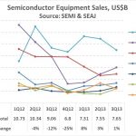
Synopsys IP Designs Edge AI 800x100

Full Chip IR Drop Analysis using Distributed Multi Processing

Full Chip IR Drop Analysis using Distributed Multi Processing
by Daniel Payne on 07-02-2013 at 6:56 pm

IR drop analysis across your board, package and SoC ensures that your Power Delivery Network (PDN) is robust, and that your system will function to spec. There are both static and dynamic approaches to IR drop analysis of a full-chip with billions of transistors, while the dynamic approach produces the most accurate results compared to silicon behavior. Apachehas been providing IR drop analysis tools for about a decade now, and Aveek Sarkar spoke with me this afternoon about how they have used Distributed Multi Processing (DMP) to scale up the analysis.


Aveek Sarkar, Apache

Continue reading “Full Chip IR Drop Analysis using Distributed Multi Processing”


Globalization of Semiconductor Manufacturing Industry

Globalization of Semiconductor Manufacturing Industry
by Daniel Nenni on 07-02-2013 at 3:00 am

The following is a brief summery of an article co authored by SemiWiki member Apek Mulay.It is definitely worth a read when you get a chance:

Globalization of Semiconductor Manufacturing Industry: From Deception to Reformation Towards Recovering US Macro-Micro Economic Losses


During the recent recession (since 2007), many observers wrote the American Manufacturing Obituary, claiming that America could no longer be regarded as a world leader because of intense competition from low-cost competitors. Trade liberalization has increased the economic interdependence among nations. Multi-National Corporations (MNCs) in US have established operations in developing counties where labor is cheaper. One consequence of this increased Globalization of manufacturing industry has been movement of jobs and production from U.S. to Low Labor Cost (LLC) countries (which are often less developed countries) for higher corporate profits. This practice is called Offshoring, and is a direct consequence of Monopoly Capitalism, where the prime motive is corporate profits without consideration of job losses for people in the home regions. Globalization works to the detriment of American workers and reinforces unfair labor competition because of lower wages and inadequate working conditions existing in developing nations. In this article, we focus on electronics and semiconductor industry, its moving offshore and causing loss of jobs and R & D in it, and offer some insights into:

  • The causes of the loss of global dominance of US Electronics and Semiconductor industry over years;
  • How to fix this problem, that can contribute towards rejuvenating our economic growth;
  • How to revive the employment market associated with this industry.

‘Globalization’ was conceived to enable American companies to enter other countries’ markets and thereby enhance US economic dominance. However, this has resulted in a backlash and now found to be clearly a deceptively defective economic policy, which has resulted in loss of dominance of US economy and transferred the dominance to LLCs like China. The acute unemployment in US caused by ‘Globalization of Manufacturing Industry’ needs both (i) short term fix in order to rejuvenate its electronics and semiconductor industry, and (ii) long term fix to avoid such an economic blunder in future.

Strategic government policies with respect to education, workforce training, tax reform, trade reform, economic reform and immigration reform can have considerable influential effect in attracting both domestic and international human capital to in turn promote innovation. Such policies can rejuvenate the industry by spurring innovation and world class R&D and also prepare the work force for future.

By modifying Capitalism to work for 99% (along with 1%) would enable employees to become the primary share holders in US companies (instead of the Wall Street stock holders), the CEOs of companies would have to make decision jointly with the employee representatives on the Management Board in best interest of their employees and hence of the companies. Thus, the hard work of employees would bring higher incomes through profit sharing. This kind of a co-operative economic system based on Mass Capitalism would preserve incentive to growth, and avoid undue pressure from investors on Wall Street to ship jobs overseas for getting higher return on investments. This economic system would ensure prosperity to all Americans with a sustainable economic demand and minimize malpractices which lead to economic bubbles. This system would also ensure that wages of hard working Americans catch up with their productivity with minimal government interference.

lang: en_US


A Brief History of VLSI Technology, part 1

A Brief History of VLSI Technology, part 1
by Paul McLellan on 07-01-2013 at 8:15 pm

VLSI Technology was founded in 1981 by Dan Floyd, Jack Baletto and Gunnar Wetlesen who had worked together at Signetics. The initial investments were by Hambrecht and Quist, a cross between a VC and a bank, and by Evans and Sutherland, the simulation/graphics company.

The fourth person to join the company was Doug Fairbairn. He was still at Xerox PARC but went to interview the three founders for Lambda Magazine that he was just getting off the ground. He immediately realized that their plans for a foundry wouldn’t really work without a new generation of design automation tools because the EDA tools of that era were polygon-based layout editors but semiconductor technology was already past the point where you could reasonably design everything by hand.

In the early days of VLSI, the company was sustained by designing ROMs for the first generation of video game consoles, which were all cartridge-based. Each cartridge actually contained a ROM with the video-game binary programmed into it. The fab in San Jose was not yet up and running, and so these were actually outsourced to Rohm in Osaka Japan. In parallel, Doug hired a bunch of PhDs, many from Carver Mead’s Silicon Structures Project at CalTech, and the profits from video games were invested in a suite of tools for what we would now call ASIC design, although that name didn’t come until later.

An early project, called Bagpipe, was to design a chip for the not-yet-announced Apple Macintosh. This chip had more sound channels and better graphics than the Mac eventually had, but Steve Jobs canceled the project in 1982 since he worried that finishing it might make the Mac late, which is actually laughable in retrospect since the Mac came out in 1984 at least a year later than planned in any case.

VLSI had a fab on McKay Drive in San Jose. At the time, it was the only high tech building there, surrounded by greenhouses growing flowers and, across the street was the Chrysanthemum Growers Association Hall that was sometimes used for company-wide meetings. The first process brought up was 3um HMOS, followed by 2um CMOS and 1.5um CMOS.

Fairly early on the investors decided that the company’s management team was too inexperienced to manage the anticipated growth. Al Stein was brought in as CEO. The company went public in February 1983, still not yet profitable, and almost immediately afterwards the 3 original founders departed.

The initial design technology, still based largely on the Caltech/PARC ideas in Mead and Conway’s seminal book Introduction to VLSI Design, was a mixture of manual design with generators for basic structures such as registers and adders using an internal language called VIP. The focus of the tools was on verification with a DRC, circuit extractor, LVS (called netcompare), simulators (VSIM, with no timing and then TSIM which had timing based on a simple capacitative model).

However, designs were getting too large for this approach and despite the inelegance compares to Mead and Conway’s ideas, it was clear that layout had to be much more automated. So standard cell libraries and a full place & route system were developed along with schematic capture to input the design.

In order to be successful, design had to get closer to the customer. Initially this meant that the customer came to VLSI and there were several teams working on site at VLSI’s San Jose buildings. For example, the main chip in France Telecom’s initial implementation of Minitel was created by Telic (now buried somewhere in Alcatel-Lucent) who sent a team of engineers from Strasbourgh to San Jose for several months.

The next step was to create a network of Design Centers (DCs) initially in the US, and then also in Japan and Europe, since it was clearly not scalable to bring all the customers on-site to California.

The IBM PC was now in its high growth phase and many customers of VLSI were designing products for that market (modems, add-in peripheral cards) or designing chips to create PC clones. In fact there were dozens of companies working with VLSI with a business strategy of being a large percentage of the PC industry, obviously an impossibility for all of them to succeed. To serve this market, VLSI developed the first of what today is called semiconductor IP although VLSI called them megacells (and later functional system blocks or FSBs). These included all the standard components in a PC such as the UARTs or the 6845 graphics controller.


Dan Yoder, as an experiment over a weekend, put all of these megacells together onto a few chips and created the first PC chipset, a chipset that could be used to create a full PC along with the Intel microprocessor and memory. VLSI ran with the idea and built up a large business in PC chipset standard products to go with its mainline ASIC business. One generation of chipsets was even resold by Intel.

Two key EDA products in the late 1980s were the datapath compiler and the state-machine compiler, effectively one of the first synthesis tools. The datapath compiler could take a complex description for a datapath and quickly generate a fully laid out datapath on silicon, using its own optimized custom library, not standard cells. And the state-machine compiler could take a description of a state-machine (or just any old logic) and produce an optimized implementation in standard cells. Together these two tools made creating complex designs much easier.

Part 2


Smartphone Shipment Explosion Sustained by $50-$75 devices, Mostly in China

Smartphone Shipment Explosion Sustained by $50-$75 devices, Mostly in China
by Eric Esteve on 07-01-2013 at 9:21 am

Until recently, talking about smartphone incredible shipment growth was understood as shipments of A5 iPhone or Galaxy Note, and this was true. Devices priced at $500 or more are shipping like baguette in Paris, but this fact is only true in Europe, Korea, Japan or USA. Does that means that people living populated countries like India or China don’t like smartphones? In fact, they can’t afford paying for Apple iPhone or Samsung Galaxy, but they also want to be equipped, thus they buy affordable Android devices, at a $50 to $75 price range. Thanks to these new consumers, the smartphone market is continuing to explode in term of devices volume, even if the overall growth in value is more modest.

The printed value in the above picture are not in US$ but in Yuan Renminbi, so “300” is equal to about $50. Such prices look pretty low when comparing with what we pay in western countries, isn’t it? There should be good reasons behind. Let’s have a look at the 2G Baseband chip price evolution in the picture below. In 2008, most of the phone sold were Feature phone and not yet smartphones, just starting to ship. 2G Baseband IC were selling for about $5, Nokia was still the leader, as well as TI with 41% share of this DSP based chip market, and CEVA, selling DSP IP core to chip makers designing 2G Baseband, had a modest 11% market share. In 2012, everything has changed: IC price has been cut by 50%, TI market share is down to 1% (!), and CEVA is dominant with 63% share. When cutting IC price by 2, it become easier to build a very low cost phone! Another very interesting remark is the fact that the “old” DSP chip is almost dead, at least in the Wireless market, and has been replaced by a DSP core, opening the way for larger integration, as the Baseband chip can be itself integrated into a larger multi-purpose device, the Application Processor…

But you are thinking: “OK, but you don’t build smartphone with 2G Baseband, rather with 3G IC”… which is completely true! That’s why it could be wise to take a look at the 3 G Baseband IC price evolutions:

Another miracle, explaining the smartphone crazy adoption, is the fact that 3G IC price has also been cut by 2, going from $14 in 2008 down to $7 in 2012, but only for TD-SCDMA technology, precisely the technology supported in China, when the UMTS/W-CDMA (supported in USA and Europe) 3G IC price has decreased by a mere 10%. There are several consequences that we can review. The first one is that smartphone price is not going to drastically go down any soon for people like me, buying in Europe, or for those buying in the USA. The second is that we now understand why smartphone devices can be sold for such a low price in China, thanks to the 3G IC cost decrease. The latest is the market analysis we can make: Qualcomm market share has gone up to 45%, before decreasing to 39% when Samsung has decided to change 3G IC supplier, and will more likely decrease in the future, even if we don’t expect Qualcomm to do as bad as TI did. This competitive analysis also gives a very good indication about CEVA market share, constantly growing from 19% in 2008 up to 30% in 2012, and most probably expected to grow again in the future. Why? If you take a look at CEVA customer base, you list: Spreadtrum, Broadcom, Intel… and if you compare this list to the 3G Baseband IC suppliers to Chinese OEM manufacturing smartphones, it’s a perfect fit!

This latest picture show the 3G smartphone devices market share in China: Samsung is the clear leader (buying 3G BB IC to a combination of Spreadtrum, Broadcom and Intel, depending on the phone type), followed by a trio made of Lenovo, Coolpad and Huawei (buying 3G BB IC to a CEVA customer), then by many OEM enjoying smaller market share, out of which Nokia, again using 3G BB IC integrating CEVA DSP IP core. It took to CEVA more than a decade to be a DSP leader, but the company is likely to stay long, as the S/W associated with the various Modem have been validated on the long term. As a result, CEVA’ customer can enjoy short Time-To-Market, and a lower cost of ownership than when buying to Qualcomm or developing in-house DSP.

Eric Esteve from IPNEST

lang: en_US


When Atrenta celebrates with STM and CEA-Leti in Grenoble

When Atrenta celebrates with STM and CEA-Leti in Grenoble
by Eric Esteve on 07-01-2013 at 3:20 am

Grenoble is French city well-known within the Semiconductor industry to be one of the last location counting wafer fabs, not only in France but in fact in Europe. Back in the 70’s, under French government impulse, through the Commisariat à l’Energie Atomique (CEA) and the LETI subsidiary in charge of Electronic related research, the first wafer fab have been built in Grenoble, developing 5 micron MOS technologies. Almost 50 years later, there are still wafer fabs in Grenoble, processing wafers in 28 nm or even less. In the meantime, a complete ecosystem has emerged around CEA-LETI and ST-Microelectronics, counting companies like SOITEC (Silicon on Insulator wafer production) and several EDA start-up, most of them being hosted into a location called Minatec (please don’t ask me for the meaning of the acronym!). Atrenta is probably too old to be called a start-up, as the success of their flagship SPYGLASS product has put the company on the EDA forefront. When Atrenta has decided to create an Engineering team in charge of developing from scratch power dedicated EDA tools, they could have extended their Sri Lanka or India operations, they have started this new product line development in Grenoble instead.

Last week, there was a party organized at Minatec, celebrating the two years anniversary of Atrenta implantation in Grenoble. If you consider that this party was a wine degustation, including:

  • Chablis (Chardonnay) as a starter
  • Crozes-Hermitage (Red wine, Syrah)
  • Saint-Joseph (same)
  • Condrieu (Vionnay)a wonderful white wine!
  • To end with Cotes-Rotie, my preferred Cotes du Rhone…

How could I have escaped attending to such an event!

It was also an opportunity to meet with the complete Atrenta Grenoble team, pretty young engineers for the most, coming from all across Europe, as well as with managers from LETI and ST-Microelectronics, and obviously Atrenta, as Ajoy K. BOSE, Chairman and CEO was there, demonstrating that Atrenta is really committed to this Grenoble implantation! It was also an opportunity to hear a talk and meet with Philippe Magarshack, Executive VP at STM. In fact, I saw this name appearing in so many events and conferences that I thought it was a myth, but I can now guarantee that he is real, and very open to talk, especially if you speak about FDSOI (if you remember, I talked about FDSOI in Semiwiki a while ago)… Philippe is second from the left, when Ajoy is right on the middle on the above picture.

On the above picture, you can see that wine and networking are going well together!

Last point, Mike Gianfagna, Vice President of Corporate Marketing at Atrenta, commenting about the success of this Grenoble implantation, pointing the fact that it’s the first time, and first location in the world, where the conjunction of politic willingness, government backed program like MINATEC, semiconductor industry (STM) and advanced research (CEA-LETI) allow the emergence of such a R&D project that Atrenta has realized, and “simply works fine”.

Eric Esteve from IPNEST

lang: en_US


Workload-tuned cores seeing greater interest

Workload-tuned cores seeing greater interest
by Don Dingee on 06-30-2013 at 10:00 pm

Is it possible to design a processor with very high performance and low power consumption? To answer that, embedded illuminati are now focusing on designs tuned to specific workloads – creating a tailored processor that does a few things very efficiently, with nothing extra.

Continue reading “Workload-tuned cores seeing greater interest”


The Future of Mobile Semiconductor Devices

The Future of Mobile Semiconductor Devices
by Daniel Nenni on 06-30-2013 at 5:00 pm


During my trip to Taiwan I hopped on over to Hong Kong for a speaking engagement. One of the things I do as an “Internationally Recognized Industry Expert” is help the financial world understand the semiconductor landscape as it pertains to SoCs and mobile devices. Usually I do this over the phone or in writing but I prefer to do it in person whenever possible. Nothing compares to the human connection with eye contact and a firm handshake. The Q&A part is my favorite since I get to ask questions too.

I generally start with a brief history of the fabless semiconductor industry then talk about specific technologies in use today, the major players in the market, and where I see them going forward. The examples I use are from my work with the top fabless semiconductor companies, the foundries, and the design enablement ecosystem (EDA and IP). That takes about 45 minutes I then open it up for questions. The big question is what will happen to the semiconductor landscape in the coming years? For me, the “coming years” means the coming semiconductor process nodes, 20nm, 16nm, and 10nm.

Mobile devices will continue to drive the semiconductor industry into the foreseeable future, no surprise there. 28nm was a bit of a shocker when TSMC was the only semiconductor manufacturer to yield which resulted in an unheard of > 90% market share. This caused shortages and the highest wafer margins we will probably ever see. Critics blame TSMC for the 28nm shortage but let’s face facts, the other foundries did not yield as forecasted and TSMC did not build capacity for > 90% market share.

20nm will be a half node since 16/14nm (20nm with FinFET transistors) is only one year behind. FinFETs offer significant power savings so the mobile people will be FinFETing as fast as they can. The high performance companies will probably skip 16nm to focus on 10nm which will arrive two years later. If you are betting against these dates be sure and hedge those bets because you will lose. The fabless semiconductor ecosystem is a force of nature, there is no stopping it now.

As it stands today there will be (6) foundries manufacturing FinFETS: Intel, Samsung, TSMC, GLOBALFOUNDRIES, UMC, and SMIC. If they all yield, which is a big IF, there will be a serious glut of FinFET wafers on the market. Even if only Intel, Samsung, and TSMC yield, which is NOT a big if, there will be a wafer glut. A softening global economy will put even more pressure on wafer pricing.

So what happens next? A price war of course, a price war of epic proportions, a game changing price war that will benefit the mobile market and the fabless semiconductor ecosystem but will change the foundry landscape for sure. Who will win the price war? Samsung of course. Samsung is no stranger to wafer dumping, which is how they dominated the DRAM market. Samsung is dominating the mobile market in the same manner, by flooding it with product. Samsung’s goal is to be the #1 semiconductor company and I honestly believe they will be.

Let’s not forget Intel was once a dominant player in the memory market. Unfortunately increased manufacturing competition from Asia dramatically reduced margins. As the story goes, Intel’s Andy Grove and Gordon Moore are talking about a board meeting the next day. “What do you think would happen if they fire us?” Grove said. “They’ll hire someone who’ll get us out of memories” Moore replied. “So why don’t we walk out of that door, come back in and do that ourselves.” And they did.

I cannot think of a more exciting time in the history of semiconductors. TSMC creating the fabless semiconductor ecosystem 25 years ago was exciting but FinFETs and the plethora of low cost mobile devices that are coming ranks right up there!

lang: en_US


Today’s Program is Brought To You by the Letter A

Today’s Program is Brought To You by the Letter A
by Paul McLellan on 06-28-2013 at 9:09 pm

What do nVidia, Freescale and GlobalFoundries have in common? They are semiconductor companies? They are ARM licensees? They are doing 28nm chips? They all have the letter ‘a’ in their names?

All true, but that’s not what I was thinking of. But the letter ‘a’ is a clue since Apache (and Ansys) begin with ‘a’. All three companies have issues with various aspects of semiconductor power that they look to Apache to help them address. Is there anyone designing chips who doesn’t have issues with power? Of course not. Which means that everyone would benefit from another connection, that in the next few weeks they are all doing Apache webinars about power, noise, power reduction, reliability, and power delivery network analysis.

Apache, a subsidiary of Ansys in case you’ve forgotten, is the de facto standard for pretty much anything in the power area, from high-level early analysis at the RTL level down to the most accurate post-physical-design analysis of the entire power network from board, through the package and onto the chip.

All three customers presented at the Apache booth during DAC a few weeks ago. But if you couldn’t make it to Austin then you can see what you missed (although I don’t think you’ll get a cute toy dog).

First up is nVidia on July 16[SUP]th[/SUP] at 10am Pacific talking about Early RTL Power Analysis and Reduction for Advanced Power-Efficient GPU Designs. This webinar covers nVida’s methodology for RTL power analysis and reduction using PowerArtist. Material presented will include RTL vs sign-off power correlation, runtime performance metrics, and specific examples of power reduction techniques applied and results achieved. Register here.

Next is Freescale on July 23[SUP]rd[/SUP] at 10am Pacific on Power, Noise and Reliability for Advanced Automotive and Networking ICs. This webinar covers experiences of SoCs for Automotive and Networking Applications. Instead of discussing typical Power and Rail Analysis details, this presentation will focus on insights gathered from running analysis and silicon results, and will include power analysis (RTL and gate-level), rail analysis (static and dynamic), handling complicated IPs and standard cells, ESD signoff and cell electromigration analysis. Register here.

And on August 6[SUP]th[/SUP] at 10am Pacific, GlobalFoundries will talk on Hierarchical Voltage Drop Analysis for Complex Power-Gated, Multi-Domain 20nm Designs. This webinar will cover a hierarchical IR drop analysis flow using Totem to trace networks of over 800 multi power domains through switch cells, and to generate sub-block abstracts that can be used for top-level analysis, allowing a large speed-up of IR drop analysis in comparison to flat analysis. Registerhere.

More details of the webinars including links for registration are on the Apache website here.

DAC news: The ACM/IEEE A.R.Newton Technical Impact Award in EDAwas awarded to Keith Nabors of Apache, who co-authored (along with Keith White) the paper FastCap: a Multipole Accelerated 3D Capacitance Extraction Program. He received the award at the DAC 50[SUP]th[/SUP] Awards Dinner on the Wednesday evening of DAC. The paper was picked because of its impact on the industry but Keith probably had a hard time remembering much about it since it was published over 20 years ago when he was at MIT. If you want to read the paper it is here.


Design Test and Regression Management of SoCs

Design Test and Regression Management of SoCs
by Daniel Payne on 06-28-2013 at 2:26 pm

Eric Peersfounded Missing Link tools in 2008 and his company was acquiredby Methodics in 2012, so I met with him at DAC to understand how their EDA tools for Design, Test and Regression Management are used in an SoC design.


Eric Peers, Methodics Continue reading “Design Test and Regression Management of SoCs”