llmda newsletter ad (2)

Two New ESL Tools for Power and Thermal at DAC

Two New ESL Tools for Power and Thermal at DAC
by Daniel Payne on 05-27-2014 at 6:47 pm

Gary Smith published a list of what to see at DAC, and I noticed that he listed DOCEA Power in a category of ESL Thermal. I’ll be meeting the DOCEA engineers on Wednesday at DAC to learn more about their two newest ESL products:

  • Thermal Profiler
  • Power Intelligence

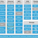
In general DOCEA Power tools allow you to manage power and thermal analysis at the ESL level, which is a higher level of abstraction than RTL or gates. This ESL approach can:

  • Save 40-70% on power consumption by early power architecture exploration
  • Secure your specification and avoid design re-spins
  • Improve power and thermal budget tracking all along the design
  • Speed up power and thermal management software validation and debug

deFacto Technologies and DOCEA are making a joint presentation on Monday, June 2 at 5PM in Room 258/260:

  • Joint design flow to fill the gap between architecture and RTL during low-power design exploration

Pascal Vivet from CEA-LETI is presenting in Session 16 of the Design Track on Tuesday, June 3 from 10:30AM – 12:00PM in Room 105:

  • Thermal Modeling Methodology for Fast and Accurate System Level Analysis. Application to a Memory-on-Logic 3D circuit.

On Thursday, June 5 at 9AM to 5PM in Room 202 there’s a workshop:

You can visit DOCEA at DAC in booth #2223, and look for my blog next week. To schedule a DAC meeting, use this online form.

Docea Power develops and commercializes a new generation of methodology and tools for enabling faster more reliable power and thermal modeling at the system level. Based on its Aceplorer platform, the Docea Power solutions use a consistent approach for executing architecture exploration and optimizing power and thermal behavior of electronic systems at an early stage of any electronic design project. The company is headquartered near Grenoble, France, and in San Jose, CA, and has sales and application support offices in Japan and Korea.

lang: en_US


Different Approaches to System Level Power Modeling and Analysis for Early Design Phases

Different Approaches to System Level Power Modeling and Analysis for Early Design Phases
by Daniel Payne on 05-27-2014 at 3:14 pm

At DATEthis year in Dresden, Bernhard Fischer from Siemens CT(Corporate Technology) has presented an interesting summary of the various techniques used for power modeling and analysis at the architectural level. He went through the pros and cons of using spreadsheets, timed virtual platforms annotated with power numbers and a dedicated system level power modeling tool (Aceplorer). He also had an example application (a signal processing design) to show results mostly using the two latter approaches.

We mostly agree with the outcome of the study, and we encourage any person interested in power modeling at the architectural level to ask for a copy of the slides. I would like to add to the presentation a few points collected through my experience, working with Docea Power customers.

One general observation is that early power estimates are due way before any virtual platform is available. Most companies use a power model to answer Requests for Information (RFI) or Request for Quotations (RFQ) with statistical use case descriptions or dynamic representations of the most important use cases. Power architects are of course interested in the availability of a timed virtual platform as it provides a way to get a better use case representation, but they can’t wait till it is available, so they need to have a model of their own. Besides, power estimations need to take into account a complete device, not just the most important functional blocks, and this often includes analog and RF blocks and voltage regulators. Adding the different non-functional power consumers to the Virtual Platform further delays its delivery (which is mostly developed at the usage of system architects and software teams) and makes it more difficult to debug.

Another observation is that power architects expertise is not on functionality and SystemC coding and compiling, but rather on modeling the power behavior of blocks (leakage vs dynamic), on describing power management schemes, and on estimating the impact of different power reduction techniques. One core aspect we have found is to track power numbers (and indeed for a complex design there is a lot of data to manage), in order to be able to explore quickly any new configuration requested.

From a practical point of view, power architects have to perform a number of what-if analyses, to explore the best configuration on the number of power domains and voltage clustering. This is true for most complex designs today. To enable this exploration, power architects need an easy representation of supply rails and power domains definition. This is natively supported in Aceplorer as the tool is dedicated to power modeling. The methodology allows getting very accurate results as described in this paper from Jongho Kim (Samsung SLSI) presented at DAC 2013.


Our approach with regards to the link with virtual platforms is to get the best of both worlds! Virtual Platforms are an excellent way to describe the use cases. Whenever a virtual platform is available, with the right timing information and simulating meaningful use cases for the power architect, the activity of blocks can be monitored, captured in traces and used to describe use cases in Aceplorer. With this approach, the non-functional blocks are represented only in the power model, where they are needed and not in the virtual platform where they don’t add value.

The Aceplorer model is probably going to be pre-existing the virtual platform and a specific team in charge of its development and maintenance. The two models can be put in sync and we have demonstrated last year at DAC a mechanism to even have the virtual platform drive the Aceplorer simulation and get power and temperature feedback. This mechanism is ideal to develop and debug optimized power and thermal management policies and provide with more accurate leakage power numbers and better what-if analysis capabilities. This is in my humble opinion, how to get the best of both worlds…

Docea Power exhibits at DAC (booth #2223). If you are visiting the show in San Francisco next week, visit our booth to learn more.

Written by: Ridha Hamza, DOCEA Power

lang: en_US


The Chip Design Game at the End of Moore’s Law

The Chip Design Game at the End of Moore’s Law
by Paul McLellan on 05-27-2014 at 2:58 pm

I just came across and interesting video from last year’s Hot Chips conference. Dr. Robert Colwell of DARPA discusses how the processor design industry is likely to change after it becomes too difficult to continue scaling transistors to ever-smaller dimensions. This is likely to occur sometime within the next decade, so companies need to be planning for the transition today.

Today Dr Colwell heads up programs looking into promising future technologies, but his talk draws a lot on his many years at Intel as a CPU architect. He even points out that CPU microarchitecture has been pretty ineffective. Since he started designing processors that ran at 1MHz the performance has improved 3,500 times due to improvements in semiconductor performance. Due to changes in how processors are architected (pipelines, branch prediction, caches etc) maybe just 50X.

The big challenge is that CMOS has been such a wonderful technology and we have had a free ride. Until recently every process generation is faster, more area, lower power and lower cost. It is an exponential that has gone from his boyood 6-transistor radio to multi-billion transistor chips today. In future the improvements will be much less from process generation to generation. If we have to live with architectural improvements primarily then progress will be very slow. Of all the technologies that DARPA is looking at, he has about 50. But he reckons that only 2 or 3 are truly promising.

He sees 7nm as being the end of the road and Moore’s Law is over around 2020 or 2022. Worse, Intel actually makes all its real money moving its processors into the next node and if 5nm is not coming or is too expensive then designing in 7nm is less attractive.

He has on one of his slides something that I’ve said for some time: When Moore’s Law ends it will be economics that stops it, not physics. Follow the money.

This has implications for many industries that are fed on semiconductors. For example, almost all improvements in cars for ages have been things like engine control units, navigation and so on. Basically processors. So improvements in cars will get a lot slower.

In case the video above doesn’t work then it is here.


More articles by Paul McLellan…


SEMICON West 2014 Preview

SEMICON West 2014 Preview
by Paul McLellan on 05-27-2014 at 12:46 pm

There is a really big conference coming up in San Francisco…no, not DAC although of course that is coming up too. I’m talking about SEMICON West which is much bigger, filling all 3 Moscone exhibit halls. It is July 8-10th. It is, of course, the semiconductor equipment industry (and solar) show.

The opening keynote on Tuesday is by Mark Adams, the President of Micron. I am sure one of the things that he will talk about is the Micron Hybrid Memory Cube (HMC), one of the very first 3D chips to go into volume production. It consists of 4 DRAM die on top of a base logic die.

The Wednesday keynote is The Art of the Possible: How Manufacturers are Leveraging Digital Technologies to Drive Business Transformation in a Connected World by Sanjay Ravi of Microsoft where he is the Worldwide Managing Director, Discrete Manufacturing Industry.

One of the most interesting areas at SEMICON is always the TechXPOTs which are two on-the-exhibit-floor presentation areas. Every morning and afternoon there are sessions for some particular area that is hot right now with 6 or 7 presenters from different companies.

TechXPOT south on Tuesday has Next Generation MEMS in the morning and Variability Control in the afternoon. on Wednesday the session that most interests me is in the morning on Supply Chain Challenges for 10nm and Beyond. Then in the afternoon it is Productivity Solutions for 300mm and Smaller. Finally on Thursday it is 3D Printing in the morning and Breakthrough Research Technologies in the afternoon.

TechXPOT north is on Testing into the Future on Tuesday morning, the Future of 3D NAND Flash in the afternoon. Wednesday morning is Bringing Silicon Photonics in Production and then in the afternoon Automotive Innovation. On Thursday morning Disruptive Compoun Semiconductor Technologies.

Also, new this year, is the semiconductor technology symposium STS. This is a comprehensive technology and business conference addressing the key issues driving the future of semiconductor manufacturing and markets, aligned with the latest inputs from the ITRS. Discover the trends shaping near-term semiconductor technology and market developments in areas including 450mm, advanced processes and materials, lithography, packaging, and test.

The website with full details, registration and more is here. Registration is discounted until June 6th.

SEMICON West is the flagship annual event for the global microelectronics industry. It is the premier event for the display of new products and technologies for microelectronics design and manufacturing, featuring technologies from across the microelectronics supply chain, from electronic design automation, to device fabrication (wafer processing), to final manufacturing (assembly, packaging, and test). More than semiconductors, SEMICON West is also showcase for emerging markets and technologies born from the microelectronics industry, including micro-electromechanical systems (MEMS), photovoltaics (PV), flexible electronics and displays, nano-electronics, solid state lighting (LEDs), and related technologies.


More articles by Paul McLellan…


Mark Milligan Joins Calypto. Plus Google at DAC

Mark Milligan Joins Calypto. Plus Google at DAC
by Paul McLellan on 05-27-2014 at 12:07 pm

I talked to Mark Milligan this morning, who has just joined Calypto as VP Marketing. I first met Mark back when he was at CoWare and I was at VaST or maybe it was Virtutech. Then he moved on and ran marketing at SpringSoft which, I’m sure you remember, Synopsys acquired. I asked him what encouraged him to join Calypto.

He said that there is a lot of technology that has been brewing for years. When Mark was at the Open SystemC Initiative (OSCI) he said that synthesis from C was the holy grail. But back then the technology was immature. The other big problem was that there wasn’t a very good verification flow. Having simulated everything at the C (or SystemC) level it all had to be resimulated at RTL to make sure that the high level synthesis had done its job.

Four things have changed in the intervening years:

  • High level synthesis technology in Catapult has got really good
  • The sequential equivalence checking (SLEC) technology that Calypto originally developed has got to be good, so that now there is a formal verification flow
  • Power has become the dominant constraint in algorithmic design, and in the FinFET era dynamic power in particular
  • The complexity of the designs that people are doing using this technology is mind-boggling

The approach is not applicable to every type of IP, often there is legacy RTL or that RTL is simply the right level to do the design. But modems often have changing specifications, graphics is always about improving the algorithms. By being able to simulate the design at the C or SystemC level there is a huge gain in performance. But the biggest thing driving adoption is that there is serious pain in some of these areas and an RTL-based approach doesn’t work. It is simply not possible to iterate designs fast enough, to move them from one process generation to the next and so on.

At DAC, Calypto have customer presentations on how companies are using the products to do these types of design. Calypto have 3 products. The Catapult high-level synthesis (that came from Mentor originally). The sequential logical equivalence checking (SLEC). And the PowerPro sequential power reduction technology. Catapult and PowerPro allow design to be done at high-level and SLEC gives a corresponding verification flow.

But the big coup is that Google will be presenting how they use Catapult for design of video processors, that they call VP9. By doing it at the C level they can share code with partners in a quasi-open-source way. Their partners can also feed improvements back to Google. Further, by moving up to the C level it is much easier for “software types” to do hardware design. It is all about being able to take the algorithm and efficiently implement it in silicon (either and FPGA or gates or even just run it on a processor) and meet the power budget.

Calypto’s DAC booth is #2333.


More articles by Paul McLellan…


Methodics @ #51DAC!

Methodics @ #51DAC!
by Daniel Nenni on 05-27-2014 at 11:00 am

This is the biggest year ever for Methodics at DAC, with lots to show, and a team of people excited to talk to customers and potential customers alike. Methodics will also be giving away Pebble Smartwatches!

Methodics theme for DAC2014 is “IP and design management done right”. A key part of this message is to show how their unique open approach which includes open interfaces, open architecture, and open data – not only helps customers and partners, but also sets them apart from the competition who focus on the traditional closed approach of EDA companies to lock customers into there solutions.

At their booth Methodics will be demonstrating ProjectIC – their lifecycle management platform, and VersIC their analog design data management platform.

For ProjectIC they will have three demos that match to the different use models of the platform:

  • ProjectIC for Digital Design: Focuses on the design collaboration, release management and automatic bad release rejection aspects of ProjectIC. These capabilities of ProjectIC allow designers to focus on core elements of design without the need to become DM and release experts. Bad release rejection ensures that a bad check-in by a single designer does not stall the whole development team.
  • ProjectIC for Integrators: Shows how ProjectIC simplifies complex integration of modern SoC’s containing 10’s or 100’s of IP. Ccentral and shared configurations help teams stay coordinated, while hierarchal release and bug tracking means changes to underlying IP are propagated automatically (and correctly) up the design.
  • ProjectIC for Enterprise IP Management: Follows the lifecycle of an IP and shows how the ProjectIC connects IP creators with consumers. A dynamic IP catalog is seamlessly integrated into a designers workspace to show the real-time status of the IP, while IP caching builds on capabilities in the underlying DM and file systems to make all IP appear local to designers and deliver real-time workspace creation even for designs that pull IP from multiple repositories around the globe.

For VersIC they have a unified demo that shows DM and release management seamlessly integrated into the analog design environment (Cadence Virtuoso for the demo, but Synopsys Custom Designer is also supported) as well as their new verification management capabilities.

Beyond the demos, there are a number of other activities they are involved in:

  • IP Track Panel Discussion– Monday 4:00pm : The panel will discuss whether next-generation highly configurable IP is breaking design and verification. Other companies in the panel are Google, Codasip, and Duolog
  • Cadence Theater – Tuesday 12:30 pm : Presents how Methodics IP and design management solutions seamlessly integrate into Cadence’s analog, digital, and mixed signal design environments.
  • ChipEstimate IP Talks – Wednesday 1:30pm : Explores the lifecycle of the IP and what is needed at each stage in the lifecycle.

Throughout DAC they will be running a daily giveaway of a Pebble SmartWatch to a random person seen with their DAC button (above). The buttons can be collected at the Methodics booth (#1407).Methodics delivers state-of-the-art semiconductor data management (DM) and IP Lifecycle management for analog, digital and SoC design teams. Methodics clients for analog and digital designers integrate natively making capabilities seamless to users. Building our solutions on top of standard Subversion and Perforce infrastructure ensures data is safe, always available, and that the tools can take advantage of the latest advancements from the software configuration management community. Methodics highly scalable and industry proven solutions are ideal for small specialized IP design teams, as well as large multinational, multisite, SoC design teams.

More Articles by Daniel Nenni…..

lang: en_US


Dark Silicon

Dark Silicon
by Paul McLellan on 05-26-2014 at 5:29 pm

One of the problems with chips today is that of so-called “dark silicon”. We can put massive functionality on an SoC today. A billion transistors, and that is just at 28nm. But power constraints (both leakage and dynamic power) limit how much of the chip can be powered up at any one time. In some cases this is not that big an issue: if your cell-phone is not making a call then don’t power up the transmit/receive logic. But in other cases it is a huge problem. There is absolutely no point in putting a 16-core processor on a chip and then finding that 10 is the maximum number of cores that can be on at any one time. The cores are identical, so it is not like the transmit/receive logic case that I just mentioned.

At the Linley Microprocessor Conference a couple of weeks ago, Drew Wingard, the CTO of Sonics presented on this, although the presentation was actually called Power Management Advances for Heterogenous Mobile Systems although as a marketing guy I prefer to talk about the problem of dark silicon

They see it as an opportunity for further power optimization. One of the thing a network-on-chip (NoC) buys you is that the power management can be much more automated. The NoC “knows” if a block is powered down when a message arrives for it and can buffer the message, power up the block and then deliver it. This makes it possible to do much more aggressive power management without depending on the embedded software people, who barely understand how the chip works, to do it through flipping register bits.

There are also lots of chip-level techniques for reducing power. Reduce the clock frequency. Turn the clock off when nothing useful is being done on that part of the chip. Power down the block completely. But for all these to be done safely it all needs to be architected into the IP. There are huge savings but it is very hard to get at them , for example, with a standard bus-based fabric: the bus must be powered if any of the attached cores are on and then the internals of the block may be powered off or not be being clocked.

The alternative approach taken by Sonics is to use the network to enable power domains. The network itself can also be partitioned inside power domains. With intelligence in the network it is much easier to shut down power domains safely and automatically wake up components by holding traffic and then sending a request to the system power manager.

SonicsGN is a power-aware on-chip network that can cope with all this. For example in the above diagram the network handles the SoC for a tablet computer including domain partitioning, clock gating and domain on/off control. This enables much finer grained power control, is safer, requires less CPU overhead and all sorts of other benefits (not least that because it is in hardware the CPU might not even need to be on). Potentially these approaches can save half of the total SoC power consumption.


The Silicon ATM

The Silicon ATM
by Paul McLellan on 05-26-2014 at 4:52 pm

One of the things that eSilicon does is handle all the backend operations for the designs that they do. eSilicon is a fabless ASIC company and so the most visible part of the business is the design (not to mention IP which is a critical input into design these days). But another key part is arranging with foundries like TSMC to get the wafers manufactured, then a test and packaging house which may be in another country, and finally delivering the designs to wherever they are going to be used.

eSilicon has an entire production management system to do this. It allows the customer to see what is going on, allows eSilicon employees to control it, and over a longer time horizon do things like yield analysis. But eSilicon wants to go further and make it so it is self-service. The ATM for silicon. No standing in line for a teller.

The first step started late last year was automatic quoting for MPW shuttles at TSMC, GF, UMC, SMIC and more foundries coming soon. I already wrote about this. There is an online form for doing your own quote and even an iPhone app. 150 different users have used the system to do over 400 quotes. I’m not sure if that excludes people like me playing with the system.


The breakdown is an interesting little bit of data in its own right. Half the quotes were either 40nm (110) or 28nm (105). The rest were more evenly spread in larger geometries all the way up to one quote at 500nm (or 0.5um as we used to call it way back when).


The next step, that is being introduced for DAC, is eSilicon’s IP MarketPlace. This allows users to search eSilicon’s IP library by foundry and technology, do what-if PPA analysis and download and configure it. There will be demos during DAC and the system will be rolled out later this year.


Next step will be full GDS-II quoting, not just for MPW runs. This will let you create a fully customizable GDS-II handoff quote online by technology, flavor, metallization, process options, package, test time, test platform, yields, production ramp, and more

  • eSilicon stands behind the online quotation, which includes NRE and production unit pricing
  • Customers benefit from a no-compromise experience
  • High level of customization
  • Instantly available, detailed and binding quotation
  • Customers are able to conduct trade-off analysis and explore a number of options
  • Not feasible without online technology

Again this will be demoed at DAC and released later in June (for TSMC).

So come by the eSilicon booth #512 and see these products being demoed. And if you time it right, you might get a free copy of Fabless, the must-have accessory this June.Plus we will be signing them at Tuesday night’s reception (and if you just happen to see us on the show floor).


Cadence Go (war-game) strategy

Cadence Go (war-game) strategy
by Eric Esteve on 05-26-2014 at 8:19 am

I was attending to CDN-Live in Munich last week, so I was expecting Cadence to announce new IP related acquisition like Lip-Bu Tan did last year (Cosmic Circuit, Evatronix and Tensilica). In fact, Lip-Bu was not in Munich and Charlie Huang, SVP Worldwide Field Operations and System & Verification Group, was holding the morning keynotes for Cadence. The announcement of immediate availability of DDR4 PHY IP built on TSMC 16FinFET process is certainly an important milestone, as the Memory Controller market segment has became the largest of the Interface IP last year, passing $100 million revenues… but it’s not like claiming the acquisition of an IP vendor like Tensilica!

Listening to presentations leaves your mind some spare time, and I was thinking about Cadence IP strategy, and about Cadence global strategy. I am sure that Wall Street would love to hear that one of the Top three EDA and IP giant has decided to buy one of the remaining two, like Cadence buying Mentor Graphics for example. Wall Street would love it because it’s easy to understand (number #2 buy number #3 to become number #1) and because a lot of money and shares are moving fast (even if you get a few % of the deal, the larger the deal, the larger your commission). But if you are not working at Wall Street but within the electronic industry, trying to understand what are the dynamics of this industry, you quickly realize that such a merge is likely to lead to a disaster. There are probably a lot of redundant products, as well as redundant peoples, and these two companies have a strong company culture-but not the same!

Thus I tried to qualify Cadence’s strategy, at least since Lip-Bu has become CEO. In respect with IP, after Denali (expensive) acquisition in 2010, Cadence has moved fast since 2012 to build small companies to enlarge the Interface IP port-folio up to the level of the direct competitor, Synopsys. Tensilica acquisition is not a cheap one, but it’s certainly a cleaver one, as Cadence is now #3 in Processor IP, leaving Synopsys/ARC far behind. Many IP vendor acquisitions at an affordable price, like putting Go stones on the playing area, sounds like deploying an old war-game strategy issued from a well-known Chinese game, the Go, but maybe the Go has been issued from war proven strategies, I don’t know. Anyway, deploying a Go-like strategy maybe the winning move in the EDA/IP industry.

The above picture is the proof that I have given a presentation during CDN-Live. I am very happy of the quality of the audience during this presentation, as I had many relevant questions, including from Intel (I guess the former Modem/BaseBand Infineon group). If you want to figure out the scope of my presentation, just take a look at the picture below, the red lines designing the scope of IPnest research.

Just as a reminder: Interface IP up-front licensing business represent today 35% of the overall licensing IP business!!

Eric Esteve from IPNEST

In the “Interface IP Survey” you will not only find the detailed IP sales results by protocols (DDRn, USB, PCIe, SATA, MIPI, Ethernet, HDMI, DP), and by vendor, but also market intelligence (IP vendor competitive analysis, market trends) by protocol, and a 5 years forecast.

More Articles by Eric Esteve…..

lang: en_US


IBM and GLOBALFOUNDRIES Deal!

IBM and GLOBALFOUNDRIES Deal!
by Daniel Nenni on 05-25-2014 at 10:10 am

An interesting deal was announced last week, another piece in the What is Next for GlobalFoundries? puzzle. IBM is sending up to 200 employees from their East Fishkill R&D facility to GF’s Malta R&D center in Saratoga County. The first thing that comes to my mind is 10nm! Considering GF is licensing Samsung 14nm, what else could it be?

GlobalFoundries has confirmed a contract with IBM in which technical workers now based at the East Fishkill plant will work for eight months at GlobalFoundries’ Fab8 chip plant, the Poughkeepsie Journal reported exclusively Friday. “I don’t know of anything else like this,” said Richard Doherty, research director at Envisioneering Group in Seaford, Nassau County. “There is nothing else like it I know of in the chip industry, or with IBM, where there’s been this transfer of talent.”

Last month The Wall Street Journal started the “IBM Semiconductor is for Sale” conversations citing unnamed sources (gotta love those unnamed sources):

Globalfoundries Inc. has emerged as the leading candidate to buy International Business Machines Corp.’s semiconductor-making operations, said people familiar with the matter. IBM also held talks with chip makers Intel Corp. and Taiwan Semiconductor Manufacturing Co., the people said, but TSMC has dropped out of the talks. While Intel is still involved, Globalfoundries appears to have a stronger interest, they said.

Last year IBM’s Semiconductor business shrank to less than $2B and is expected to shrink again this year to less than $1.5B so time is running out unless it is to be an asset sale. After talking to friends at Intel, TSMC, and IBM about this I have to agree that GF is the most likely candidate of the three. While TSMC could certainly benefit from having manufacturing facilities in the US, I highly doubt that they need the IBM semiconductor technology. Intel seems to be even less likely unless they just want to keep the technology away from the others.

As I mentioned before, the new GF CEO, Sanjay Jha, is a very clever man and knows the fabless semiconductor ecosystem:

Santa Clara, Calif., January 6, 2014 — Building on the successful track record of its first five years in the semiconductor industry and its continued commitment to build out its global network of manufacturing facilities, GLOBALFOUNDRIES announced today, from its new offices in Silicon Valley, Sanjay Jha has been appointed as the company’s new Chief Executive Officer. Jha has served as CEO of Motorola Mobility Inc. and as the COO of Qualcomm Inc.

Something big is cooking at GF, absolutely. Hopefully we will learn more about it next week at the 51st Design Automation Conference where thousands of semiconductor professionals will meet, collaborate, commiserate, and get signed copies of “Fabless: The Transformation of the Semiconductor Industry. I hope to see you there!