llmda newsletter ad (2)

Context Aware Library Models for Improved Static Analysis Accuracy

Context Aware Library Models for Improved Static Analysis Accuracy
by Daniel Nenni on 05-30-2014 at 10:00 pm

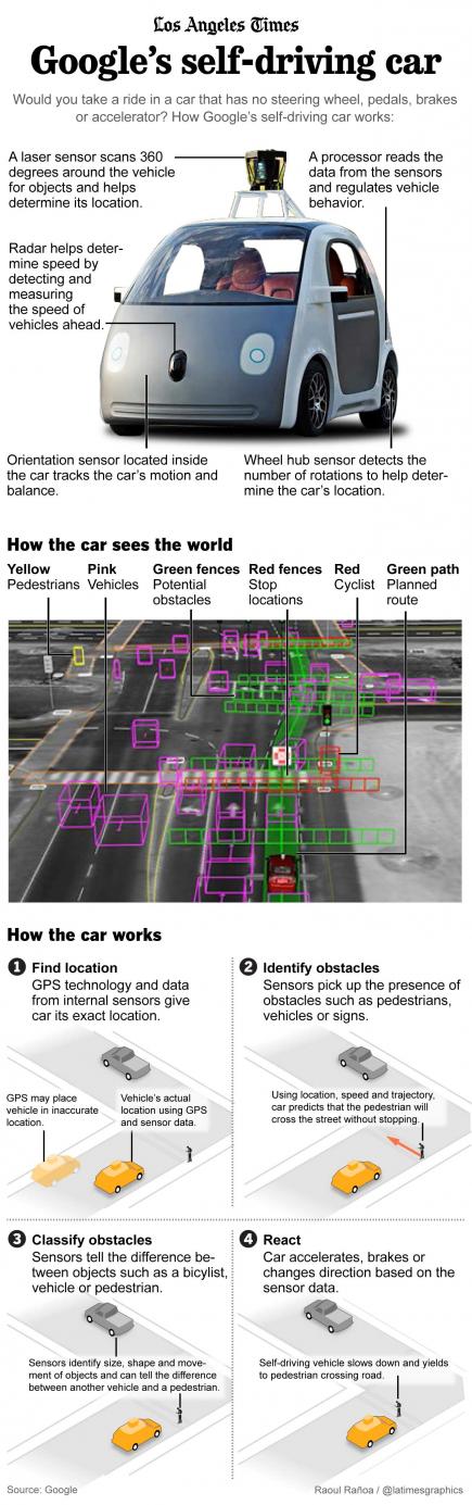
Digital semiconductor design flows predominantly use library models (typically verilog and liberty formats) for static analyses. Design sizes continue to grow and geometry continues to shrink. Demand for superior performance continue to increase. Accuracy of the library models has become more critical than ever before to enable the optimum design performance, power and noise. A library cell can be instantiated in a variety of different design context and different instances might perform differently. The idea of “one model fits all instances”, with no knowledge of design context, is a source of gap between the actual characteristics of a cell vs. those represented by the library model. A library model that is too conservative leads to over design whereas a progressive models leads to correlation issues. The EDA vendors have been struggling to provide library cell models that can represent all possible usage scenarios. At the same time traditional approaches are reaching their limits and proving to be insufficient to meet today’s design requirements.

Before we go into more details of what is lacking in library characterization softwares currently available from various EDA vendors (vs. what do today’s designers ideally need from their EDA vendors), it will be worthwhile to understand the bridge these library models create between static and dynamic analysis methods.

Dynamic analysis methods do actual simulation of the design to measure the functionality and various characteristics with high accuracy. Dynamic analysis methods however are heavy users of the compute resources and take long run times.

Static analysis methods on the other hand are inherently faster, since they avoid dynamic simulation. Instead, they use library models of the cells created by dynamic simulation. Static analysis is used for exhaustive and conservative analysis of one design metric (static timing, noise, power etc.) with no regard to design’s other metrics.

Some advantages of static analysis are:

  • It exhaustively covers the whole design.
  • It has ability to perform multiple modes in the same session.
  • It is many orders of magnitude faster than dynamic analysis.

Some of the disadvantages of static analysis are:

  • It may lead to false negatives for improperly constrained designs.
  • Static results are conservative, meaning it may flag a false problem such as negative slack because of a false-path for static timing analysis.


Modern characterization softwares pay no attention to the design context i.e. how the cells are used in the design. Ignoring the design context while creating library models, is the prime source of inaccuracy in the models that eventually leads to miscorrelation and other inaccuracies in static analysis flows. There are a number of subtle nuances (parameter and methods) that a characterization software should be aware of – as depicted in Fig1.

The ideal solution is to create/interpolate models on the fly on a need basis by timing, power, noise and other analysis software. Analysis software has complete knowledge of the context it is operating in. Analysis software spawns characterization API with correct set of inputs derived from design context. Characterization API, in turn, creates and returns model for every unit during timing, power and noise analysis.

In an ideal world, this solution works perfect. However, in the world of limited resources, it runs into issues including performance degradation by many orders, large compute resources requirement, large number of software license required, and lack of incentive to analysis software providers to adopt this methodology- just to name a few. Figure 2 depicts this perfect (but highly impractical) flow with analysis, characterization and simulation, generating models with real design context.

I was impressed by Paripath’s library characterization platform that produces CAM(Context Aware Model) models that not only meets today’s designers’ accuracy needs but also uses massive distributed processing to efficiently conquer the run-time and capacity challenges. The main concept behind their solution is to allow the characterization software to study a representative design and collect set of parameters/methods suitable to design type, constraints and technology node among others. Armed with design context information, Pa!path’s characterization software uses circuit analysis and simulation to generate models as depicted in Figure 3. These models not only have knowledge of what is inside the cell, they are also aware of the context they’ll be used during static analysis methods.

Paripath’s characterization software armed with design context information is capable of generating models that are context aware. Context aware models are best equipped to address difference in philosophy and technology of dynamic analysis and static analysis methods. These context aware models aid to provide true design sign-off with good correlation of static analysis to circuit simulation. Context aware models help designers avoid the over- and under-design of designs reducing costs and saving time from design schedules.

Written by Rohit Sharma

lang: en_US


Google Robot Cars are Coming!

Google Robot Cars are Coming!
by Daniel Nenni on 05-30-2014 at 10:30 am

Paul McLellan and I attended the 2014 Embedded Vision Summit in Silicon Valley this week. The most interesting session for me was on the new Google car that was announced earlier in the week. But first, to set the stage, let’s look at a new study by the National Highway Traffic Safety Administration (NHTSA) that shows motor vehicle crashes had an $871 billion economic and societal impact on U.S. Citizens, which is the equivalent of 1.9 percent of the $14.96 trillion Gross Domestic Product (GDP) in 2010.

NHTSA’s new study, The Economic and Societal Impact of Motor Vehicle Crashes, 2010 cites several behavioral factors as contributing to the huge price-tag of roadway crashes based on the 32,999 fatalities, 3.9 million non-fatal injuries, and 24 million damaged vehicles that took place in 2010. Key findings include:

  • Drunk Driving: Crashes caused by drivers under the influence of alcohol accounted for 18 percent of the total economic loss due to motor vehicle crashes and cost the nation $49 billion, an average cost of $158 for every person in the U.S.
  • Speeding: Crashes involving a speeding vehicle traveling over the posted speed limit or too fast for conditions accounted for 21 percent of the total economic loss and cost the nation $59 billion in 2010, an average cost of $191 for every person in the U.S. Including lost quality of life, these crashes were responsible for $210 billion or 24 percent of the overall societal harm caused by motor vehicle crashes.
  • Distraction: Crashes involving a distracted driver accounted for 17 percent of the total economic loss and cost the nation $46 billion in 2010, an average cost of $148 for every person in the U.S. Including lost quality of life, these crashes were responsible for $129 billion or 15 percent of the overall societal harm caused by motor vehicle crashes.
  • Pedestrians and Bicyclists: Crashes involving pedestrians and bicyclists accounted for 7 percent of the total economic loss and cost the nation $19 billion in 2010. Including lost quality of life, these crashes were responsible for $90 billion or 10 percent of the overall societal harm caused by motor vehicle crashes.

The safety issue is near and dear to my heart as I was run down while riding my bike by a distracted driver and left for dead on the side of the road. Thankfully first responders happened by shortly thereafter and I lived to ride again.

The thing I love about Google is that they thrive on disrupting Big Industry and make quite a large amount of money in doing so. They certainly changed the search and the advertising industry similar to the way ARM brought Intel to its knees with low power/low cost processors enabling the mobile devices that have displaced traditional PCs. Apple is also one of my favorite disrupters.

The Google presenter was Nathaniel Fairfield. Nathaniel has a PhD from Carnegie Mellon University. Carnegie Mellon is known for robotics which is what we are really talking about here. Paul or I will write about this in more detail when the slides are available but this infographic is a good start:

More Articles by Daniel Nenni…..


Sidense NVM IP clears TSMC9000 at 28nm

Sidense NVM IP clears TSMC9000 at 28nm
by Don Dingee on 05-29-2014 at 7:00 pm

Maybe I’ve spent too many years whiffing solder flux fumes and absorbing doses of X-band radiation in anechoic chambers, but I’m a firm believer in the axiom: “Give me enough engineers, and I can get 10 of anything to work right, once.” We have to make this … fit into this … using only this stuff … is what legends are made of. Continue reading “Sidense NVM IP clears TSMC9000 at 28nm”


SemiWiki Exceeds One Million Users!

SemiWiki Exceeds One Million Users!
by Daniel Nenni on 05-29-2014 at 11:00 am

SemiWiki was launched on January 1[SUP]st[/SUP] 2011 and according to Google Analytics we have officially exceeded one million users (unique visitors). I really don’t know what to say but, WOW, that is a LOT of people reading SemiWiki articles, wikis, and forums (there are now 13,464 posts on SemiWiki).

According to Alexa.com SemiWiki is ranked as the 130,975[SUP]th[/SUP] most popular website in the world and 34,758[SUP]th[/SUP] in the United States (Google is #1, FaceBook is #2). That is simply amazing to me, I would have never imagined that large of an audience when I started a WordPress blog five years ago. Crowdsourcing really does work!

It was slow going when SemiWiki first started. In the first three months (Q1 2011) we only had 20,608 users but by the end of the year we had 170,501, so that was good pretty, right? My WordPress site “Silicon Valley Blog” had about 10,000 readers at its peak. SemiWiki ended 2012 with 459,608 and at the end of 2013 we had 829,408. Since other websites in our industry don’t publish their user numbers I will assume we are doing a pretty good job.

According to Alexa.com we still have a long way to go to catch EETimes which is rated the 30,949[SUP]th[/SUP] most popular website in the world and 18,160[SUP]th[/SUP] in the United States. It really is an apples to oranges comparison since EETimes is a network of websites but it serves as a good benchmark for future growth, absolutely.

In the other Alexa metrics however SemiWiki does quite well:

How engaged are visitors to semiwiki.com?

  • Bounce Rate 36.00%
  • Daily Pageviews per Visitor 5.40
  • Daily Time on Site 10:33

How engaged are visitors to eetimes.com?

  • Bounce Rate 67.60%
  • Daily Pageviews per Visitor 1.77
  • Daily Time on Site 2:15

If you are interested in learning more about SemiWiki or New Media in general I would be happy to share my thoughts with you. We can have a formal discussion on “Managing New Media” or we can just meet over coffee and chat about it. If you are not in Silicon Valley I’m a big fan of Skype and constructive criticism is always welcome.

The biggest difference between SemiWiki and other industry websites is that we all have day jobs. We are semiconductor professionals and consultants who enjoy writing and communicating the value proposition of the fabless semiconductor ecosystem. Please see our LinkedIn profiles to learn more about us as individuals:

If you want to be successful with SemiWiki you need to give us two things: Access and honesty. As semiconductor professionals our time is limited and since we trade on our reputations honesty is an absolute requirement. As bloggers we share our experience, opinions, and observations so you may not always agree with what we write but you should however see value either way.

The most important thing you should consider about New Media and SemiWiki specifically is going for the long game versus the short one. Don’t just jump in and out of our lives with news releases. Work with us, develop relationships, and integrate SemiWiki into your long term communications strategy, absolutely.

More Articles by Daniel Nenni…..

lang: en_US


TSMC: Keynote, OIP, 20nm, 16nm, panels, and more #51DAC

TSMC: Keynote, OIP, 20nm, 16nm, panels, and more #51DAC
by Paul McLellan on 05-28-2014 at 8:11 pm

What is TSMC doing at DAC?

The biggest event is presumably Cliff Hou’s DAC keynote on Monday at 3.25pm Industry Opportunities in the Sub-10nm Era. And he also wrote the foreword to Fabless, the book that Dan Nenni and I have written and where you can get a signed copy on Tuesday evening at the reception.

There is an IP workshop Driving Quality to the Desktop of the DAC Engineer which takes place on Sunday from 1-5pm in room 202 in the Moscone Center. This is presented by Steven Chen and Lluis Paris.

TSMC is participating in two panels. The first is on the IP track and is in room 101. Lluis Paris is moderating the topic of IP Quality. There is also a pavilion panel on Connecting Everything: Architecting the Internet of Things,Dan K is on the panel.

There are lots of presentations with TSMC’s partners, too many to mention.

TSMC themselves are on booth 1801. They will be talking a lot about IP quality. Have you noticed TSMC are very big on IP quality? They started just using software tools such as Spyglass for evaluating quality but they have now created a silicon validation lab in Taiwan to take it to the next level.


So the top level message is:

  • 20nm Complete

    • In mass production
    • Everything qualified and validated on customer designs
  • 16nm FinFET Complete

    • V1.0 Certification completed
    • IP silicon validated and available
    • Interface IP in silicon validation now
    • 16nm FinFET will be ready by end of year


One new thing you might not have heard is that there is a new 28HPC process offering. Spice corners have been tightened and there is a new signoff methodology. There is also a new high-efficiency 7-track library.

OIP is thriving. It has been running for over 12 years. The portfolio is impressive with over 7000 titles from 40 different IP vendors.


Overview of activities is here. Theater schedule on the booth is here.

Once again, TSMC’s booth is #1801.


More articles by Paul McLellan…


How About a Quality-Aware IP Design Flow

How About a Quality-Aware IP Design Flow
by Daniel Payne on 05-28-2014 at 6:18 pm

In the EDA world we use hyphens quite often to describe our technical approaches, like: DFM-aware, Power-aware, Variation-aware. I just read a white papertoday on the topic of Quality-Aware IP Design Flows, written by Fractal Technologies. If your group creates IP or re-uses IP, then there’s always the question about the readiness or quality of each IP block. Shown below is a flow of how cell libraries and larger IP blocks get created by an IP vendor and then used by an SoC designer, along with the checking and validation processes necessary to ensure high quality and reduce re-spins.

Incoming IP Inspection

An incoming IP inspection QA tool should detect any incompatibilities on new IP for your present design flow or self-consistency within the IP blocks. The earlier that you uncover an inconsistency with IP the better, because you don’t want to find an IP block issue during tape-out because of the amount of effort required to re-validate your entire SoC design. Semiconductor IP has many assets that require checking:

  • Databases
  • File formats
  • Design views (logical, physical, simulation, etc.)

The QA tool from Fractal Technologies that provides a GUI-based approach to incoming IP inspection is called Crossfire, and it has a matrix of possible checks for each IP database and file format. Any violations or mismatches may then be graphically highlighted. You can even waive any irrelevant view-mismatches for your particular SoC project as needed in order to reduce the amount of information reported.

Background IP Checking

As cell libraries and IP blocks are used within an SoC project, you should be running IP checks again in context, however they can now be run in the background instead of having to use a GUI. You only need to know if there’s been any mismatch and where it arises.


Automated development and characterization flow, all steps are push-button, QA should also be push-button

The Crossfire tool also supports background operation through the use of a Setup API, where you have dedicated checking scripts written in your favorite language (Python, Tcl, Perl) that can automatically find recently changed databases and then run the required checks. You can integrate QA validation within your design repository, so any views that change in your working copy will run the Crossfire checks when the repository commit procedure runs. With this background IP checking approach you can later view any of the QA validation results using the Crossfire Diagnose tool.

With this background IP checking approach the SoC designers don’t have to perform any manual steps to ensure that QA checking is happening. Only when an automated check fails, does the designer need to take any action and quickly pinpoint the source of the failure using Crossfire Diagnose.

Summary

Library and IP QA checks can be run both interactively and in batch modes to ensure the highest design quality, and shortest time to market with the Crossfire tool. If you’re visiting DAC in San Francisco next week, then stop by to see Fractal Technologies at booth #507.

lang: en_US


Samsung Voice of the Body

Samsung Voice of the Body
by Paul McLellan on 05-28-2014 at 2:12 pm

I just back from Samsung’s big announcement held at the SFJazz center (very conveniently 15 minutes walk from my place). They put a stake in the ground about their program at the intersection of medicine and health and technology. They had said in advance that they would not announce any new hardware but in fact they did…although you can’t buy one yet. They were clearly going for an Apple style announcement.

Young Sohn, who is president and chief strategy officer, opened the show, talking about how the first generation was just apps on your iPhone (oops, I mean Galaxy). The second generation is fitness devices like fitbit. And the third generation will have new wearable sensors. He pointed out that your car does a better job of monitoring its health that is possible for you today.

What they decided to do was to build an open platform for development, consisting of 3 parts which they covered in some detail:

  • Simband
  • SAMI
  • Partnerships, the biggest being IMEC and UCSF Medical Center.

The big challenge is that sensors are not quite good enough yet. Consume too much power, too large, too pricey. So they built a prototype platform. The first decision was where to put it: glasses, wrist, leg, ear, chest. They decided to go for the wrist since people are used to wearing things on their wrists even though it is not the idea location for data acquisition.


The band is impressive. It looks nice. Inside is what they call the sensor “bucket” where you can put sensors so that they are against the skin. Of course there is a display and a battery. IMEC, in addition to all its famous research on semiconductor technology, is also the world’s leading biosensor research organization. There are clearly some clever sensors with multiple wavelength LEDs that penetrate the skin and can then detect movement of blood vessels, galvanic skin response, a two probe electrocardiogram, estimation of blood pressure. But anyone can build a sensor, not necessarily Samsung, and the expectation is that some startups and other experts will do so.

IMEC designed a chip that I presume Samsung manufactured. The whole board is just 14x34mm with the chip which is 28nm, has bluetooth and wireless, and a 1GHz dual core ARM. The band can be charged with a little shuttle battery that attaches (normally while you sleep) so you never need to take the Simband off.


And it is all real, not just a plastic mockup of what it will look like one day. Live on stage Ram Fish gave a live demo. You can see his heart electrocardiogram, blood pressure, heartrate, heartrate variability and more. The signals were all changing continuously on the screen projected up from the stage.


They have worked with both UCSF and with a company called physiq to be able to generate a continuous general wellness score. physiq has had success in detecting issues in heart attack patients days before the patient feels any different.

The band is not available yet but you can start to see just how big a change this sort of technology will make towards monitoring your own health and wellness, and potentially sharing data with your doctors, truly making an era of personal medicine: you rather than people like you.

The second part of the announcement was SAMI, the Samsung Architectural Multimodal Interaction (somehow I think they picked the acronym and then worked out what it might stand for). This is a cloud based system for uploading all the raw data and then allowing sophisticated massive data algorithms to derive useful insights. You, the user, is the ownder of the data and you control granting access to services. The API’s for SAMI will be available by the end of the year a the Samsung Developer Conference. The goal is to have easy access, but full security and what they call “frictionless ingestion” which sounds more like drinking a good beer.

They showed Ram’s health going up and down over the previous week depending on whether he was awake or asleep. “Looks like he was having a stressful week, I wonder why?”

To kick start an ecosystem they have ceated a $50M investment fund for sensors, software etc. Plus I recognized several VCs in the audience. Lip-Bu was in the front-row as it happens, I’m assuming with his VC hat on rather than his Cadence CEO one.

This is clearly Samsung’s stake in the ground in what I’m sure will also have entrants from Google and Apple. They want to get out ahead both in perception and in creating an ecosystem around their technology since they are the first to admit they are not health and medical experts in all areas. It is going to be interesting to watch.


RedHawk Excels – Customers Endorse

RedHawk Excels – Customers Endorse
by Pawan Fangaria on 05-28-2014 at 11:00 am

Since a few years, I have been following up Ansys Apachetools for semiconductor design, verification and sign-off. RedHawk is the most prominent platform of tools from Ansys, specifically for Power, Noise and Reliability Sign-off. It has witnessed many open endorsements from several of Ansyscustomers through open presentations, about which I have talked in the past. For a product, what can be a better promotion than its users speaking out for it? This is a win-win situation where a product earns revenue by satisfying its customers’ needs and in turn utilizes that revenue in enhancing it further to satisfy new needs of its customers, i.e. continuous improvement. One doesn’t need to go, acquire something new from the market to satisfy those needs. This philosophy is truly reflected in RedHawk’s development as I see it since last few years.

While RedHawk has been leading in the power, noise and reliability sign-off space since long, last year Ansys added significant capabilities into RedHawk by improving its capacity and performance to handle large designs with billions of transistors at sub-20nm and at very high clock speed of the order of 3+ GHz. That was a fourth generation release (with product named as RedHawk[SUP]TM[/SUP]-3DX), right in time when customers needed it. A great extension for 3D-ICs was provided which supported both concurrent and model-based multi-die simulations of designs with silicon interposer and TSVs. While simulation of all chips could be done at full layout detail, model-based approach allowed CPM[SUP]TM[/SUP](Chip Power Model) for some of the chips. A multi-tab, multi-pane GUI was provided to view and analyze voltage drop hotspots and other characteristic in the whole 3D stack at once. The sign-off accuracy and coverage was enhanced with the use of new event and state propagation engines that could be used in vector-based, VectorLess[SUP]TM[/SUP] and mixed-excitation modes, to gain maximum coverage without loss of accuracy.

This month, Ansys announced RedHawk 2014 platform which supports FinFET-based semiconductor design (along with all earlier process technology based designs). As FinFET-based designs working at low operating voltages exhibit lower noise and reliability margins, greater emphasis has been provided on accuracy of analysis. The platform has been added with ‘Distributed Machine Processing’ (DMP) capability which improves memory footprint and simulation runtime each by about 2-3x over its previous release and handles large designs of the order of billions of transistors at flat simulation accuracy.

RedHawk-CPA is another great and unique capability in the 2014 platform which provides chip-package co-simulation and co-analysis. This is done by merging a fully distributed package parasitic network with an on-die power delivery network, thus allowing the tool to provide immediate feedback on the quality of the package design as well as the impact of package parasitic on the chip performance.

A testimony of RedHawk 2014 handling tighter EM (electromigration) limits and new EM rules (such as those considering current direction, metal topology and via types for power as well as signal nets) posed by FinFETs is its certification by TSMC. In order to counter heat reliability issue, a novel concept of CTM (Chip Thermal Model) has been introduced which can very accurately capture the thermal distribution for FinFET devices and enable a thermal-aware EM analysis.

Also, ESD integrity, an important step in reliability has been enhanced by careful ESD design planning to check degraded diode protection and reduced wire capacity.

While looking at Ansys’s agenda in DACwhere they will provide more detailed views and information about this new release of RedHawk 2014 platform, I observed several of their customer presentations scheduled at DAC where the actual users of these tools will be speaking about how they were benefited from RedHawk and other tools of Ansys. It will be interesting to closely watch those presentations to know about the real value of these new enhancements in RedHawk, at least RedHawk-3DX. Of course, a few of them, if they would have used customer beta version of RedHawk 2014, may reveal about that as well.

Here are some of the important customers I noted who would primarily talk about their experience with RedHawk, results and recommendations –

Jun 2, 1:00 PMSamsung: Chip-Package-System based Power Integrity Analysis Flow for 14nm Mobile Designs
Jun3, 3:00 PMNXP: Noise Coupling Analysis for Advanced Mixed-Signal Automotive ICs
Jun 4, 12:00 PMSTMicroelectronics: Designing Smart Power-Grid with Reduced Die-Area Using RedHawk
Jun 4, 1:00 PMLSI: Silicon Correlation of RedHawk Dynamic Voltage Drop in High Power SoC for Storage Application

There are other interesting presentations by Applied Micro, Cienaand Synapse. Also, there are product specific sessions and multiple other customer presentations at various locations within DAC premises. Look at the Ansys page here for more details.

Registerfor any of these presentations. Ansys is exhibiting at booth #1413, it will be worthwhile to pass through that. Stay tuned to hear from me on details of some of these interesting presentations at a later date.

More Articles by Pawan Fangaria…..

lang: en_US


Understanding QoR in FPGA synthesis

Understanding QoR in FPGA synthesis
by Don Dingee on 05-28-2014 at 8:00 am

We’ve all heard this claim: “Our FPGA synthesis tool produces better quality of results (QoR).” If you’re just hoping for a tool to do that automagically, you’re probably doing it wrong. Getting better QoR depends on understanding what an FPGA synthesis tool is capable of, and how to leverage what it tells you. Continue reading “Understanding QoR in FPGA synthesis”


DRM2PDK: From design rule manual to process design kit

DRM2PDK: From design rule manual to process design kit
by Daniel Nenni on 05-28-2014 at 3:00 am

Exactly a year ago Sage Design Automation launched its revolutionary iDRM product, enabling for the first time to graphically capture design rules and compile them into checks automatically – no programming required. Using the graphical design rule editor, users could draw the layout topology that describes the design rule, could add measurements by drawing arrows between edges and objects and then use these measurements as parameters in a logic expression that represents the rule that needs to be kept. Once a rule has been captured in iDRM, it serves not only as a clear visual description and formal documentation of the design rule, but it also becomes an executable expression: Push a button and the design rule compiler will scan through a physical design database and will look for all instances that use a similar pattern to that design rule and take all the relevant measurements of the parameters (variables) that were used in the rule definition. The result is a complete list of all such instances, each with complete information of the relevant measurements, orientations, location, etc.


Draw design rule / View matches and errors / Get report of all values

iDRM now becomes a broad platform for anything design rules
iDRM design compiler has already been used to develop design rules, analyze them, create checks and verify DRC decks. Now, for this upcoming DAC, Sage-DA has broadened the scope and function of the iDRM platform to also include PDK parameters. At DAC, Sage-DA will demonstrate how PDK parameters for generating parametrized cells (Pcells) can be automatically created and updated from the iDRM design rule source. The iDRM platform can thus be used as a single point of entry for design rules enabling consistency and accuracy across a broad array of EDA tools and flows.

Process Design Kits (PDKs) include specific technology files for the creation of parametrized cells e.g. PCells and PyCells. Parametrized cells are widely used in custom digital, analog or mixed signal design. They are pieces of programming code that generates physical layout instances based on the Pcell parameter values. Pcells must obey to all the relevant design rules in order to generate DRC-correct physical instances. Currently, the tech files for these cells are created manually based on the information in the design rule manual (DRM). Anytime there is a change or update in the DRM, the relevant information needs to be updated in the respective Pcell technology file. This is a cumbersome and error prone process. With this new capability of iDRM, the relevant tech file parameters and resulting generated layout will be updated automatically once the DRM is updated with iDRM. This not only saves time, but it also ensures consistency and eliminates potential errors that may hinder the integrity of the physical design database.

Where to see: Demos of this new DRM2PDK capability will be held at the Design Automation Conference (DAC) on June 2-4 in San Francisco, at the Si2 booth #1107 at 12:00 PM on Monday June 2nd, and at the Sage-DA booth (#1423) throughout the exhibit hours.

Sage Design Automationprovides design rule consistency and closure between manufacturing process limitations, their respective DRM (design rule manual) representation and their DRC deck implementation.Sage-DA’s breakthrough iDRM (integrated design rule management) technology integrates an easy-to-use graphical design rule capture with instantaneous checking capability. iDRM enables non-programmers to quickly capture design rules and generate correct-by-construction checks, accelerates the development and availability of design rule checks for new process technologies and ensures their correctness and consistency, delivering higher yield and faster production ramp-up of integrated circuits (ICs) in advanced process technologies.

More Articles by Daniel Nenni…..

lang: en_US