On SemiWiki we have some 247 blogs and forum discussions on the topic of “automotive“, so I’m pleased to learn that at DAC in San Francisco there is a new track just for automotive systems and software. Just consider all of that electronic content in your typical auto:

Will IoT Drive the Next Semiconductor Revolution?

To further my quest to comprehend the latest trends in the semiconductor industry continues, I spent the morning with SEMI at the “The Silicon Valley Breakfast Forum: Internet of Things (IoT) – Driving the Microelectronics Revolution” seminar. I’m a big fan of the breakfast seminar concept. I’m up early anyway and it is nice to get out of my lazyboy command center at home and press the flesh in Silicon Valley. And did I mention the free breakfast? There is nothing like hot green tea, warm bagels, and fresh fruit to start your day, absolutely.
Internet of Things (IoT)-The network of physical objects that contains embedded technology to communicate and sense or interact with the objects’ internal state or the external environment.
By the way, if you or your company are interested in the IoT or the wearables market it would be a pleasure to meet you. I have spent a lot of time investigating this and am at the point where I can discuss it somewhat intelligently. My focus is design enablement but I’m open to discuss and strategize all aspects of IoT. Of course not everyone agrees with what I have been writing:
“Based on my research, there is no customer research or positive feedback on wearables. Quite the contrary, Samsung is taking a bath on these products. I don’t know what research you have that justifies your position that some will hit it big, unless you are just stating your personal opinion. The difference between you and me is that I actually know what the semiconductor companies are doing with their customers – not just reference designs, but real design activity. Significant design-ins for wearables just is not there.” Bill Giovino
Famous last words…. meanwhile, back in the real world, Intel is offering $1.3 million in cash grants to winners of its “Make It Wearable” competition. This is a global contest to fuel innovation by giving individuals a platform to develop real-world applications using Intel processors of course. Go Intel!
Here are some of the interesting points from the SEMI IoT Forum made by: Karen Bartleson, President IEEE Standards Association and Senior Director of Community Marketing @ Synopsys – Alfonso Velosa, Research Director @ Gartner – Kerry McGuire Balanza, Vice President of Strategy @ ARM.
What is IoT?
- Wearable Devices and the way they interact
- Meters and machines and how they manage
- Smart home/smart appliances and when we want them
- Connected cars and how they are constructed
- Smart cities and smart Governments
Semiconductor vendors will drive the IoT architecture by investing in design from devices to the cloud: MCUs, Embedded Flash + RF, Sensors, MEMS, low power, 2G/3G/4G, Bluetooth, WiFi, GPS, NFC, Zigbee, Security, and proven process technologies (not leading edge).
Expect many types of things in a highly fragmented market.
By 2017, 50% of internet of things solutions will originate in start-ups less than three years old!
The IoT Opportunity is much larger: Analysts predictions for connected devices (2020): 30 billion? 50 billion? 75 billion?
Current trend shows strong growth. Not new, it’s been around for >20 years. Connected things > world population (6.8B).
IoT scale and diversity is very different from mobile. The number of Internet-connected devices projected to be in the home of the average family of four (with two teenage children) in 2020 = 50 — up from an average of about 10 connected devices in 2012.
Recommended Reading:
• TSPs Must Invest in the Rapidly Evolving IoT Ecosystems Now
https://www.gartner.com/doc/2694117
• Competitive Landscape: Semiconductor Companies Prepare to
Battle for Supremacy in the Internet of Things
https://www.gartner.com/doc/2649018
• Definition: Operational Technology Security
http://www.gartner.com/document/2589921
• The Internet of Things Will Shape Smart Cities
http://www.gartner.com/id=2395415
• Uncover Value From the Internet of Things With the Four
Fundamental Usage Scenarios
https://www.gartner.com/doc/2485815
• Hype Cycle for the Internet of Things, 2013
http://www.gartner.com/id=2571716
• Hype Cycle for Operational Technology, 2013
http://www.gartner.com/id=2568622
Thank you again SEMI for the breakfast and opportunity to learn more about the future of the semiconductor industry!
SEMI is the global industry association serving the nano- and micro-electronic manufacturing supply chains. Our 1,900 member companies are the engine of the future, enabling smarter, faster and more economical products that improve our lives. Since 1970, SEMI has been committed to helping members grow more profitably, create new markets and meet common industry challenges. SEMI maintains offices in Bangalore, Beijing, Berlin, Brussels, Grenoble, Hsinchu, Moscow, San Jose, Seoul, Shanghai, Singapore, Tokyo, and Washington, D.C. For more information, visit www.semi.org.
Show Me How To Get Better DRC and LVS Results For My SoC Design

Most IC engineers learn best by hands-on experience when another more experienced person can show us what to do. If you cannot find that experienced person, then the next best thing is a video from an expert. I was surprised to find out that video was so important today that the #2 most viewed web site on the Internet was www.youtube.com, just behind #1 www.google.com. At SemiWiki we also believe that videos can help you to learn quicker, especially when it comes to using the popular Calibre DRC and LVStools from Mentor Graphics. We’ve setup a Wiki page of videos and here’s an overview of what you’ll learn in this series of six videos.
Running Calibre Golden Signoff within Synopsys IC Compiler
James Paris shows us how to invoke Calibre from within the Synopsys IC Compiler tool by using a GUI. Instead of running separate DRC tools at each stage (Floorplan, Power and Ground, Placement, Clock Tree Synthesis, Final Route), why not use the sign-off DRC tool within each stage. An interactive DRC run can be quickly started, and results viewed for debug using RVE (Results Viewing Environment). Any job customizations can be saved in a runset file for easy re-use in subsequent runs.
Automating Calibre Interface Configurations within Synopsys IC Compiler
Often in your IC design flow you want to trigger events before or after a DRC or LVS run, maybe send an email or run a script to categorize the types of errors and warnings reported. Internal and external triggers are introduced and explained in this video.
Improving Visualization of DRC Errors
Using Virtuoso for IC Layout the error messages from a DRC run can be obscured or hidden underneath polygon layers. The use of a Check Types Overide (CTO) file will help removed un-needed layers making DRC debug easire. To fix a DRC violation a hyperlink to the design rule manual can be created, instead of having to manually look it up.
Changing Calibre Interactive Default Settings
If you want Calibre to always run multi-threaded and with hyperscale, then you can change your default settings by creating a new defaults file by looking up the variable names. Every project team can decide what their favorite defaults should be, then use a common defaults file.
Documenting, Reviewing, and Sharing Calibre DRC Results
Saunder Peng shows how to avoid manually documenting a foundry waiver by automating the process in Calibre and creating an HTML report, saving you hours of time.
Instantly Open a Partial Oasis or GDS Database in DESIGNrev
IC layout files greater than 10GB in size can take a huge amount of RAM to load, and involve long wait times. There’s a new option in Calibre called Open Incremental, where you decide the specific area of interest instead of full detail. Just drag your cursor across the area of interest, then you can quickly view DRC errors. About a 10X to 100X speedup in loading is possible using Open Incremental.
Summary
Calibre users will save hours to time by learning from each of these how-to videos. The videos are well-edited, take less than 5 minutes, and give you instant time savings. Now that’s a good investment. Mentor has also setup a YouTube channel for IC Nanometer Design where you will find dozens of useful how-to videos.
lang: en_US
Fast & Accurate Thermal Analysis of 3D-ICs
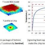
As Moore’s law started saturating on a single semiconductor die, the semiconductor community came up with the approach of growing vertically by stacking dies one above other in a 3D-IC arrangement. However, a major concern with a 3D-IC is that the heat generated by each die can get trapped in the stack, and hence it’s extremely important to accurately model the thermal map of Chip-Package-System (CPS) as a whole in order to manage the heat in a 3D-IC. Accurate thermal profiling is necessary for right placement of thermal sensors, T[SUB]max[/SUB] control and thermal-aware EM sign-off. The thermal responses are coupled with power map (especially at 28nm and below) due to leakage current in device layers and self-heating of interconnect wires. Considering the practical situations, a dynamic thermal analysis along with accounting of time factor due to thermal capacitance of the package and system can provide a realistic approach to thermal analysis in 3D-ICs.
Researchers at Apachestudied the effect of heat capacitance to the temperature rise on a chip in BGA package as shown above. In the power up transient analysis, it is observed that in the chip-package (CPS) mode, the steady state is achieved in more than 100 seconds, while in chip-only mode (i.e. ignoring heat capacitance in the materials outside the die) the same is achieved in just about 0.6 seconds, thus leading the temperature to respond quickly to power changes in chip-only mode.
A step-by-step solution approach applied on finite element (FE) model of the complex 3D-IC structure which can be quite large and can invite the solution steps thousands of times in the full thermal transient analysis, is impractical. A simple procedure to obtain temperature transient response for any location in the FE model is by using Green’s function of temperature from the step change of power on a chip. A graph of temperature response on a hot spot on chip using full thermal transient and Green’s function approach for a 40-sec power on and off in the same CPS environment shows that the results are almost similar whereas Green’s function approach is at least 60x faster. In case of larger FE models with more degrees of freedom, the difference in simulation time can be still more significant.
Apache’s chip power tools (RedHawk and Totem) can be used to compute the average power based on event-driven (if VCD file is available), vectorless (if no VCD file is available) or mixed-mode (if partial VCD file is available) approach. Chip power depends on usage which, for example for a smartphone, can be different for voice, email or streaming. In order to control power, a chip can be made to operate in different modes. A temperature sensor can be handy in sensing when the limit crosses in high-performance power mode and initiating the chip into low-performance low-power mode until the temperature drops to a desired level.
The power tools are used to generate a temperature-dependent power library called Chip Thermal Model (CTM). Using CTM, a chip thermal tool, Sentinel-TI(Thermal and mechanical Integrity) is sufficient to generate converged thermal and power results. CTMs can be hierarchical, assigned to multiple sub-regions such as blocks or clusters in an SoC and adapted to configurable stack of dies in a 3D-IC.
Stephen H. Pan, Norman Chang and Tadaaki Hitomi at Apache in their technical paperat IEEE 3DIC 2013 conference, presented testcases using the CTM and Green’s function approach to predict thermal transients at locations in a wire-bond BGA and in a 3D-IC design with flip chips.
Transients in a BGA package with 16x16mm substrate, 240 solder joints, wire-bond die of 5×5.1mm, Theta_JA range from 76 to 81 C/W and mounted on a 100x100mm 4L thermal board were calculated at several locations under different power modes. A series of power activities were applied to check the consistency of thermal wave with power activation. The temperature level for each location is affected by both the hot spot location and the overall average power level.
Above images show chip power generated with three different power modes, i.e. a CTM for each of these conditions and temperature profiles on-chip and in package along with their corresponding power map for condition #1.
Transients in a 3D-IC package (12x12mm, 6L, and 144 solder joints); with an SoC (5.2×5.2mm) at the bottom and a MEM (1.9×1.9mm) and LOGIC (2.72×2.72mm) at the top were calculated using hierarchical CTMs which are also configurable. The CTM for the whole SoC is not available because the IPs in some of the blocks do not have power map available, except the total power consumption of each block. However, part of the power on the SoC is in a cluster and its CTM can be generated. There are high and low power modes in this 3D-IC design to which the device switches according to existing temperature.
Above images show the temperature dependence of total power in the cluster and its distribution at converged temperature, and temperature profile in the 3D-IC chips at the high power mode. Thermal responses at different power modes were studied.
This methodology for 3D-IC dynamic thermal analysis is useful in the back-annotation to the individual die for accurate thermal sensor placement, T[SUB]max[/SUB] control, and thermal-aware EM sign-off. The methodology is described in more detail with several references in the actual paper. It’s an interesting read.
More Articles by Pawan Fangaria…..
lang: en_US
A Brief History of Functional Verification
Usually these brief history pieces are totally written by the SemiWiki blogger whose name is at the top. Often me since that was how I prototyped book chapters (buy). Well, OK, I did actually write this but it is completely cribbed from a presentation earlier this week by Wally Rhines who gave a sort of keynote at the announcement of Mentor’s Enterprise Verification Platform. He is the CEO, you didn’t need me to tell you that did you?
Verification started with…nothing. This was the rubylith era. You did manual design, built it, tested it, redesigned it, rinse and repeat. A friend of mine from that era said the worst thing was finding a bit of rubylith lying on the floor underneath where all the big sheets were hung. You had no idea if it was off your design and pretty much all you could do was build chips and hope.
Then transistor level simulation started with Ron Rohrer’s CANCER program. Ron seems to be a child prodigy in circuit simulation, getting his PhD before most people get their bachelors. Then the algorithms morphed into a new program, Simulation Program with Integrated Circuit Emphasis. Wait…that spells SPICE. They presented it in 1973, put it in the public domain, and within a very short time every academic department and every semiconductor company was using it and making derivatives. The basis sparse matrix algorithms survived for a long time and allowed much larger circuits than ever before to be simulated.
But larger designs required gate-level simulation. Lots of companies provided that, Mentor, Daisy and Valid (the DMV) in particular. Mentor’s solution was Quicksim. At VLSI ours was VSIM then TSIM.
In 1983 the DOD awarded contracts for the acronym within an acronym VHDL, which stood for VHSIC hardware description language and VHSIC was very high speed integrated circuit. There were other languages, most notably GHDL at Genrad, an outgrowth from Brunel University in the UK where the HILO simulator was originally developed in which it ran. Developed by Phil Moorby who would go on to develop…
…Verilog, which came along in 1985 and took off since Synopsys adopted it as the language for RTL synthesis. Cadence acquired Gateway (the owners of Verilog) in 1989 and it became an IEEE standard in 1995. Gordon Moore noted that “the only reason for VHDL was to force Cadence to put Verilog into the public domain.”
In those days simulation performance benefited from two things. Every year or so Intel upped the clock rate on the processors. But ModelSim (and other simulators have similar numbers) also improved the algorithms by a factor of 10 on top of that.
Simulator were now so fast the big problem was creating stimulus. The focus switched to methodologies. This Wally reckoned is verification 2.0. The industry, amazingly, since EDA never wants one standard when it can have three, converged on SystemVerilog. Then base class libraries were also standardized on UVM. As a result, verification has grown from $724M in 2010 to $984M in 2012 and probably over a billion now. The really big growth area has been emulation.
Emulation has gone from a very expensive option for a few groups in the biggest companies to mainstream. It is still not cheap but it is so fast that apparently the fastest simulation cycle per $ is now emulation not simulation. Plus, if you are designing a 500M gate chip, your simulation is going to take a geological timescale to complete. There is no alternative.
Chips now contain lots of software so the focus is on simulating software and hardware together. Multiple cores, huge software loads, need to boot iOS/Linux/Android/Windows before it even gets interesting. Embedded software headcount is surging. And remember that Intel giving us higher clock speeds every year. Fuhgeddaboutit. You can have lots of cores instead, which is great for DRC but not so great for simulation where everyone needs to know the time.
And formal came along somewhere during this period and, while it started off very esoteric and needed a PhD to use it and it could only handle like 1000 gates…now it is mainstream too.
So people want all these technologies to look the same. Simulation. Emulation. Formal. FPGA prototypes. Virtual platforms. A single debugger. A single code coverage database. Single. Single. Single.
That was what Mentor announced a couple of days ago. But it is a trend. Synopsys announced Verification Compiler at SNUG which is similar. And Cadence has been talking about a similar unification for the last year or so.
In a short time all the big three will have a unified verification environment that combines everything without requiring a specialist in each domain (formal, emulation, coverage, software etc) to get things up and running. Nowadays there are only design teams and they need to be self-sufficient.
Semiconductor Meme Contest!
Hopefully we all know what memes are, if not, ask one of your children or grandchildren. Having four grown children of my own I see memes posted on my FaceBook page now and again in support of my superior parenting skills. Remember when EETimes used to run a picture and readers would send in funny captions? An early form of meme, not that any of my captions ever made it in print.
According to Wikipedia:
Amemeis “an idea, behavior, or style that spreads from person to person within a culture”. An Internet meme may take the form of animage,hyperlink,video,picture,website, orhashtag. It may be just a word or phrase, including an intentionalmisspelling. These small movements tend to spread from person to person viasocial networks,blogs, directemail, or news sources. They may relate to various existingInternet culturesorsubcultures, often created or spread on sites such as4chan,Redditand numerous others in our time, or byUsenetboards and other such early-internet communications facilities. Fads and sensations tend to grow rapidly on the Internet, because the instant communication facilitatesword-of-mouthtransmission.
SemiWiki now has a Semiconductor Memes Forum in hopes of injecting humor into our otherwise “dry” profession. Since semiconductor professionals are stereotyped as “humor challenged” here is a chance to prove the world wrong.
To post a meme just enter the Semiconductor Memes forum and click + Post New Thread, pick a catchy title, insert the picture, and enter the text. The “insert picture icon” is the window with a tree in it, simple as that. You must be a SemiWiki member to post of course and you can rate the memes 1 to 5 stars using the “Rate this thread” pull down menu. A meme can be a person, product, technology, or even a company in the semiconductor industry. Be nice but be funny!
To start things out lets have a contest. Put up a semiconductor meme or add a funny caption to one of the pictures I post and someone will win a new iPad (as soon as they are available). The new iPads will be filled with 20nm silicon so that is certainly cause for celebration.
And the next time someone asks what you do for a living give them a “dry” look hold up a smartphone and say “I changed the world!”
Expert Constraint Management Leads to Productivity & Faster Convergence
The SoC designs of today are much more complex than ever in terms of number of clocks, IPs, levels of hierarchies, several modes of operations, different types of validations and checks for growing number of constraints at various stages in the design flow. As a semiconductor design evolves through several stages from RTL to layout, the constraints may change. A consistency check on the changing constraints is desired to ascertain the intent to move in the right direction. Again there may be missing constraints or incorrect constraints that must be reported in order to guide the designers to take appropriate action during the design development.
Knowing that Atrentahas a constraint management system in the SpyGlass platform that works from RTL to GDSII, I contacted Manish Goel, R&D Senior Director at Atrenta and to learn more about this system. Manish provided a detailed description about the constraint management system which is integrated into the overall SpyGlass solution framework for faster design closure. Here is the conversation –
Q: Manish, SpyGlass has a good constraint management system. Can you elaborate on its main components?
A: Yes, we have a constraint management system which is tightly integrated with the SpyGlass platform and it checks timing constraints, generates new constraints where required, verifies exceptions and manages all constraints through the complete design cycle from RTL to post-synthesis, pre-layout and post-layout stages. It checks consistency of SDC, exceptions, hierarchical constraints etc. against the design. It also removes any redundancy, identifies missing constraints, and provides guidance for cleaning delay constraints and clock definitions. The missing constraints can be automatically generated by the system. To manage the consistency in constraints, equivalence between different levels of the design and corresponding SDCs is checked. It is possible to analyze multiple modes. The tool can merge the multiple modes into a single mode. And during exception verification, false paths (FP) and multi-cycle-paths (MCP) can be verified formally, as well as based on timing. Also assertions can be generated for additional coverage.
Q: How are the constraints generated automatically? Generally RTL should come with constraints defined?
A: It is not that all constraints are generated afresh. Constraints can come from previously existing IPs or design blocks. The SpyGlass Constraints solution checks for missing constraints in the new design, reports them and generates them. For example, it can detect flip-flops (FF) not driven by any clock and it can generate a clock for them. Similarly, it can identify multiplexed inputs, clock domain crossing (CDC)and generate false path constraints at those crossings. It generates all kind of FPs including synchronous, asynchronous and quasi-static. And then it checks for correctness of all the constraints. SDC is generated incrementally as the design progresses. And that can be done through standard templates available with the initial seed file. The constraints can be identified, created and values added through intelligent wizards that can guide designers to keep the SDC correct by construction.
Q: O.K. when you talk about the constraint management, what do you exactly mean? How is the equivalence checked? How are the modes merged?
A: The constraint management provides maximum efficiency as the design evolves from RTL to layout through synthesis and P&R stages with minimum risk. See the SpyGlass constraints methodologyflow diagram above; it takes an RTL block as input along with the SDC, which can be partial. The existing constraints are checked for their correctness and completeness, the missing constraints are generated and exceptions verified (at all the stages). At this stage, multi-mode analysis is done for coverage check. At the synthesis stage, constraints are checked for synthesis readiness and functional intent is verified to match with the design intent. Also, as the gate netlist is available, the equivalence between the RTL and gate level constraints is checked. Similarly, at the floorplanning and the P&R stage, constraints are checked for STA (Static Timing Analysis) and for P&R readiness. Again, it is important to check that the functional intent matches with the design intent. At the P&R stage multi-mode analysis and merging starts. At the chip integration stage, various levels of SDC equivalence (top level vs. block level, pre-DFT vs. post-DFT, restructured RTL) are checked; there are three flavours – i) same design, changed SDCs; ii) changed designs; changed SDCs; iii) top level, block level, should have impact on timing in the same way. The complete multi-mode analysis, coverage and merging takes place at the chip integration stage. Various aspects such as constraint promotion, clocks converging on a mux etc. are taken into account.
In a typical scenario of SoCs, 70-80 modes of operations can be seen and it can be very taxing on the time to test all the modes. So, at the post-routing stage, the modes are analysed for merging and they are reduced in number. Again equivalence checking is done before and after mode-merging.
Q: How is this system differentiated from the other offerings?
A: As we talked just now, SpyGlass Constraints provides a complete integrated solution which has flexible SDC generation, formal exception verification (without needing test vectors), complete checking of SDC, multi-mode analysis and merging and a comprehensive debug system in place. There are about 300 rules covering all aspects of timing. We have patented the SDC equivalence checking. There is a unique MCP verification engine, formal clock waveform and domain verification, hierarchical methodology to support IPs and large SoCs. There are various options for most of the operations to keep the system flexible; for example, one can validate all modes of constraints in a single run and view reports per mode. This system is in production use with a large customer base since more than 6 years.
Q: How many large designs have been analysed through this system?
A: Many large designs have been taken through the system. A few customers have SDC sizes of the order of 5 to 6 GB with millions of lines of constraints and the design has hundreds of IPs. It’s not possible for designers to manage such large constraints files without the help of automated tools.
Q: Thanks Manish, that’s a great perspective you have given. One last question on the use of an existing SDC – there could be redundant legacy constraints in that, how confident would the SpyGlass Constraints tool be to remove those?
A: The tool does not remove them by itself, but it will provide all clues about the redundancy or obsoleteness of such constraints which can be safely removed. Imagine, a decision the designer finds difficult to make, the tool greatly assists in making that decision. That’s the kind of knowledge power the overall system provides.
I really enjoyed talking to Manish and learning about the intricate details of the SpyGlass Constraints solution. Considering various automated procedures, tools and techniques, flexible operations that the system employs, I can see that it definitely boosts designers’ productivity to a large extent with faster convergence of design – quicker synthesis, faster timing closure at the back-end and other stages.
More Articles by Pawan Fangaria…..
lang: en_US
4G shalt thou not count, neither count thou 2G
Five years from now, what will be the leading mobile connectivity standard? If you said 4G, please report to the brainwashing remediation center nearest you immediately. 3G is not only here to stay for the long haul, it’s growing – and will quickly become the preferred choice for M2M deployments. Continue reading “4G shalt thou not count, neither count thou 2G”
U2U: Things You Might Not Know About TSMC
At Mentor’s U2U this afternoon I attended a presentation on TSMC’s use of Calibre PERC (it is a programmable electrical rule checker) for qualification of IP in TSMC’s IP9000 program. I’ve written about this before here. Basically IP providers at N20SOC, N16FF, and below are required to use PERC to guarantee ESD is OK. This is especially critical with FinFET since the transistors are more fragile and have a lower breakdown voltage. There are also decks for 28nm but it is not required (most IP is already in volume production so problems would have shown up by now). The PERC decks guarantee that the ESD rules are all checked without the error-prone process of having to manually add identifying layers. This is the first time TSMC has specified a particular tool that must be used.
Here is a random miscellany of other facts about TSMC that I picked up:
- Risk production (samples) for 16FF was at the end of last year
- Risk production for 10FF will be end of 2015
- Lots of work has gone on on controlling capacitance on M1 and M2 at 16FF
- 10nm will have triple patterning and spacer (sidewall image transfer I assume, self-aligned double patterning). More details on 10nm at the TSMC Technology Symposium on 22nd of April
- TSMC has invested $10B a year for several years to get ready for FinFET
- FinFET challenges:
- parasitic capacitance due to the gate wrapping around the fin
- high parasitic resistance due to local interconnect M0
- quantized device sizes (only a certain number of fins)
- breakdown voltage is lower so ESD is more of an issue
- TSMC has 6600 registered IPs, adding 200 per month
- 90% hard IP is qualified through IP9000
- 100% of soft IP is qualified
- One column on IP listing is (eg) 5/25000 meaning it has been in 5 tapeouts and 25,000 wafers of production
- Extending from quality audit to slicon validation
- TSMC has set up validation centere in Taiwan
- over 20 IPs validated already (started with interface IP)
- 28nm cycle time started as 4 months, now down to 2 months
- 16nm cycle time is 5 months will probably end at 3 months
- Currently 16FF shuttle is about 160 days
- EUV, TSMC have invested $0.5B in ASML but ROI not good, keeps slipping. They are looking at e-beam and other backup strategies
- Since EUV is certainly not coming soon, 3D technologies (CoWoS) very important
What is driving N16FF. Mobile of course. Here are the changes from 2012-2014
- Display 2X
- Radio 2X
- Connectivity 3X
- AP 2X CPU, 5X GPU and 2X memory bandwidth
- 2 cores go to 8 cores
- Power same or less
- Form factor thinner and lighter
- Camera 8MP to 13MP
If you are a TSMC customer you can register for the technology symposium on 4/22 here.
Details of Mentor’s European U2U in Munich on November 6th is here. You can still submit abstracts until July 1st.
GSA 3DIC
At the GSA Silicon Summit this afternoon there was a discussion of 3D IC and 2.5D IC. The session was moderated by Javier DeLaCruz of eSilicon and the panelists were:
- Calvin Cheung of ASE (an OSAT)
- Gil Lvey of OptimalTest (a test house)
- Bob Patti of Tezzaron (semiconductor company specializing in TSV-based designs)
- Riko Radojcic of Qualcomm (you don’t need me to tell you what they do)
- Arif Rahman of Altera (FPGAs, working with Intel on 3D apparently)
- Brandon Wang of Cadence (where he is director of 3D IC solutions)
So what are the success stories? The biggest is that image sensors are all 3D ICs. Your phone contains one or two in the cameras. Other sensors are also being made but in lower volume. One reason is that there are not really power issues.
Coming next is memory on logic. Like the Micron hybrid memory cube but where the logic is the functionality of the design and not just a memory controller. The big issue is thermal. All the heat generated on the logic die has to get out through the memory die. But going forward the power using this sort of approach should be lower than the standard approach where almost all the power goes in the interface DDRx interfaces (and that roadmap doesn’t go out far). So lots of work is underway.
But others were not so sure. One problem with memory on logic is that the memory and the logic die come from different manufacturers which leads to some technical issues and also to some business issues associated with who is responsible for what. Who thins the die? Who tests the die? Who is responsible for yield loss? As compared to sensors on logic where the same company owns both.
In the EDA world, sensors on logic is not very demanding. Memory and FPGA (Xilinx is shipping 3D parts) are so regular that it is feasible to do a lot by hand. Also the cost issues are a lot less severe. Xilinx makes parts that sell for thousands of dollars and just would not yield as a single huge die. So they are saving money with 3D.
The big challenge is the true 3D system. The main driver there is connectivity. There may be thousands of signals in the sort of system Qualcomm, for example, would like to use 3D for. Tezzaron has one design with 12,000 3D connections.
The big problem, though, is cost.Calvin: “If volume goes up, costs will come down.”
Riko: “If costs come down, 3D chips will be in every phone.”
Another issue is test. You really only want to build 3D stacks with “known good die” and you have to be able to test them afterwards. This really requires BIST and self-repair after assembly to avoid too much yield loss.
So there are clearly some short-term issues of who owns yield loss. But longer term another issue is who does the R&D. Perhaps a consortium (modeled on Sematech) is needed to drive a roadmap that is out 5 or more years and to avoid building a cool solution that nobody wants.
One lesson learned: the system needs to be architected from the beginning for 3D to take advantage of it. This requires partitioning the design onto multiple die. But there is a major tool problem: there is no pathfinding tool for doing the exploration at the early stage, exploring “what if” analysis with thermal, transistors near TSVs, reliability and other issues. Nobody is creating such a tool either since it is unclear if there are more than a handful of customers that would ever use it. There is certainly not going to be any automatic tool for the forseable future that reads in one design and spits out multiple optimized chips. Today the limit is being able to read and understand more than one design at once. This allows design to be done semi-manually but for sure it does increase the risk of re-spins.
Eventually with learning the costs should come down and it should be cheaper (and lower power) to use 3D than not to use 3D.