RVN! 26 Banner revised (800 x 100 px) (600 x 100 px)

Webinar: Making Design Reuse Work

Webinar: Making Design Reuse Work
by Daniel Nenni on 04-26-2014 at 9:00 pm

Please join me for an IP conversation in collaboration with ClioSoft on Wednesday, April 30th, 2014 @ 11:00 AM PST. At the EDPS Workshop IP day there were two interesting presentations on IP reuse. The first one was by Warren Savage of IPextreme: Top Ten Reasons Why Internal IP Reuse Fails. The second was by Ranjit Adhikary of ClioSoft: Making Design Reuse Work. Take a look at the slides and let’s talk about it.


Topic: Making Design Reuse Work
When: Wednesday, April 30th, 2014 @ 11:00 AM Pacific
Presenter: Daniel Nenni, SemiWiki

Register for the Web Seminar

Who should attend

  • Managers and engineers using IP’s in their SoC
  • CAD engineers/managers

Overview
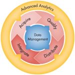
Design Reuse and IP Management are common buzz words in our industry. Yet of late, they have gained more significance with a number of companies emphasizing the need to reuse designs as much as possible.

In order to make design reuse work a number of things must be considered: Selecting the desired IP and integrating it into the design while simultaneously managing the updates to the IP is one aspect of the design flow which must be fine-tuned. It is also necessary to increase the participation of designers in creating reusable IP and provide a forum through which designers can collaborate. Finally, to further the cause of design reuse, it is important for us to move away from the traditional IP model and identify other things in the design flow which can be considered as IP. In this presentation, we will focus on how we can make design reuse work more productive.

About the Presenter
Daniel Nenni has worked in the Silicon Valley for the past 30 years with computer manufacturers, electronic design automation (EDA) software and semiconductor IP companies. Currently Daniel is a Strategic Foundry Relationship Expert for companies wishing to partner with TSMC, UMC, SMIC, GLOBALFOUNDRIES, Samsung, and their top customers. Daniel’s latest passion is the Semiconductor Wiki project (www.SemiWiki.com).

How to Attend
The seminar will be conducted via WebEx meeting service. A web URL to join the meeting will be emailed a day before the seminar. The WebEx meeting application will automatically be downloaded when you click on the URL on the day of the seminar.

Register for the Web Seminar

About ClioSoft, Inc.
ClioSoft is the premier developer of hardware configuration management (HCM) solutions. The company’s SOS Design Collaboration platform is built from the ground up to handle the requirements of hardware design flows. The SOS platform provides a sophisticated multi-site development environment that enables global team collaboration, design and IP reuse, and efficient management of design data from concept through tape-out. Custom engineered adaptors seamlessly integrate SOS with leading design flows – Agilent’s Advanced Design System (ADS), Cadence’s Virtuoso® Custom IC, Mentor’s Pyxis Custom IC Design, Synopsys’ Galaxy Custom Designer and Laker™ Custom Design. The Visual Design Diff (VDD) engine enables designers to easily identify changes between two versions of a schematic or layout or the entire design hierarchy below by graphically highlighting the differences directly in the editors.

Also Read

Importance of Data Management in SoC Verification

The CAD Team – Unsung heroes in a successful tapeout

Cliosoft Grows Again!


Digital, Analog, Software, IP – Isn’t it all just the same?

Digital, Analog, Software, IP – Isn’t it all just the same?
by Daniel Payne on 04-25-2014 at 8:31 pm

Designing an SoC requires a team, and the engineers typically use lots of specialized EDA software and semiconductor IP to get the job done. Many have started to ask about how designing a chip is different than designing and managing a large software project, or how is analog design different than digital design in terms of managing the design process. To help clarify and contrast the similarities and differences between hardware and software design I had an email discussion with Vishal Moondhra, VP of Applications at Methodics,a company that has focused on semiconductor design management for analog, digital and SoC design teams since 2006.

Continue reading “Digital, Analog, Software, IP – Isn’t it all just the same?”


Dr. Morris Chang: A Conversation with the Chairman

Dr. Morris Chang: A Conversation with the Chairman
by Daniel Nenni on 04-24-2014 at 10:00 pm

There are moments in one’s career that are memorable beyond others, and last night was one of those moments for me, absolutely:

Stanford University President John L. Hennessy will lead a discussion with Stanford Engineering Hero Morris Chang, an innovator and entrepreneur who revolutionized the semiconductor industry by creating the world’s first dedicated silicon foundry, Taiwan Semiconductor Manufacturing Company or TSMC.

The NVIDIA Auditorium at the Stanford Huang Engineering Center was filled with semiconductor executives, alumni, and students alike. I don’t know how an invitation made its way into my inbox but I am very appreciative. The conversation was engaging to say the least and quite funny at times.

Not surprisingly, NVIDIA CEO Jen-Hsun Huang did the introduction and shared some personal stories about Morris. This was reminiscent of the discussionthey had at the Computer Museum seven years ago which was used as research for the soon to be best-selling book Paul McLellan and I wrote.

Jen-Hsun started out with, “The world is full of successful people but heroes are rare”which I think fits perfectly. He also pointed out that everybody is in possession of two things: Air and products made from TSMC wafers. Jen-Hsun poked good-hearted fun at Morris but the Chairman had the last laugh, definitely.

The first question from John was if Morris had any idea of the impact TSMC would have on the world. Morris replied that at the time, TSMC was providing a solution that was waiting for a problem since the fabless companies at that time were comfortable with using IDMs for wafer manufacturing. He added that the problems came very quickly and Jen-Hsun was one of those problems! Meaning of course that NVIDIA was a fabless company that was looking for a manufacturing partner with integrity and one they could trust not to compete with them. The laughter in the auditorium acknowledged much more than that of course.

John’s second question was about TSMC’s focus on R&D. This rings true to me as I see Intel and Samsung spending billions of dollars on marketing obfuscation while TSMC focuses on R&D. The financial ratio I would like to see is R&D/marketing spending knowing full well TSMC would shine.

The Chairman responded by pointing out he had 30+ years of semiconductor experience (mostly at TI) before starting TSMC . In his words, “You have to climb to the top of a building and look at all of the available roads before you build a new one.” I have climbed a few buildings myself and find this to be very insightful.

The next question was about the Chairman’s education. Morris spent his first year at Harvard before transferring to MIT to study mechanical engineering. Morris admitted to failing his PhD exam twice at MIT before attending Stanford which again brought laughter. During his career at TI Morris was sent to Stanford to get his PhD in electrical engineering. His career goal was to be CEO, which was not possible at TI, so he joined General Instrument but decided he did not want to be CEO so he founded TSMC.

The next question was about how TSMC was launched. The Taiwan government was instrumental in funding TSMC providing 48% of the required capital. The additional investments came from Philips Semiconductor and Taiwanese investors who knew little or nothing at all about semiconductors. Morris approached Intel, TI, and semiconductor companies from Japan but they all said no. The Chairman’s memory is clear on this, naming people who actually said no such as Craig Barrett who later became Intel’s CEO.

The follow-up question was about Japan and why they are no longer major players in the semiconductor industry. According to the Chairman, Japan failed at the future. Instead of embracing the fabless semiconductor business model and unleashing innovation Japan clung to the IDM model and failed. The rest of course is history as most Japanese semiconductor companies are TSMC customers

The question I had for Morris was if he is working on an autobiography. Morris wrote a book in the 1990s which was quite successful in China. Unfortunately it did not translate well into English so it was not published here. I knew the answer to the question was no before I asked but I wanted to plant the seed anyway. It is a book I would read, absolutely. I would even write it.

When I decided to write a book my first thought was to write one about Dr. Morris Chang and how he unleashed innovation that changed the world. Friends at TSMC however suggested that I instead write about Morris’s life work which resulted in “Fabless: The Transformation of the Semiconductor Industry”, which is now available on Amazon as a paperback or in Kindle and iBook format on SemiWiki.

Morris admitted he still smokes a pipe but sited research that says pipe smokers live longer because it helps your mood (laughter). At the end of the event The Chairman was taking pictures with students so I talked to his wife Sophie. Morris always credits her for her support, and one thing I can tell you is that she is as charming as she is beautiful.

More Articles by Daniel Nenni…..

lang: en_US


Strong 2014 for Semiconductor Equipment and CapEx

Strong 2014 for Semiconductor Equipment and CapEx
by Bill Jewell on 04-24-2014 at 9:00 pm

Spending on semiconductor manufacturing equipment is headed for healthy growth in 2014. The latest data from SEMI and the Semiconductor Equipment Association of Japan (SEAJ) shows March 2014 three-month-average billings for semiconductor manufacturing equipment were up 16% from February 2014 and up 31% from a year ago. Bookings were up 16% from February and up 18% from a year ago. The March book-to-bill ratio dropped to 0.93 due to a 46% surge in billings versus February from the SEAJ data. However the book-to-bill had been above 1.0 for the previous 15 months. In December 2013 SEMI forecast 23% growth in the 2014 semiconductor equipment market. The data through March indicates the industry is on track to achieve the SEMI forecast.

The robust growth in semiconductor manufacturing equipment in 2014 implies strong growth in overall semiconductor capital spending. However the guidance provided by the largest capital spenders in the industry point to lackluster growth. The three largest spenders (Intel, Samsung and TSMC) account for over 50% of industry spending. None are indicating significant growth in spending in 2014. Intel’s guidance ranges from a 2% decline to 7% growth, averaging 3% growth. Samsung expects 2014 semiconductor capital spending to be similar to 2013. TSMC’s guidance ranges from a 2% decline to 3% growth, averaging 1% growth. The average expected growth spending by the three companies is 1%. IC Insights’ March forecast was 8.4% growth in semiconductor industry capital spending. Gartner’s April forecast was 5.5% growth. Gartner forecast semiconductor capital equipment spending would grow 12.2% in 2014, about twice the rate of overall capital spending but about half the growth expected by SEMI.

[TABLE] border=”1″
|-
| style=”width: 654px” | Semiconductor Capital Spending Forecasts, US$ Billion
|-
| style=”width: 228px” | Company
| style=”width: 60px” | 2013
| style=”width: 72px” | 2014
| style=”width: 96px” | Change
| style=”width: 198px” | Comments
|-
| style=”width: 228px” | Intel
| style=”width: 60px” | 10.7
| style=”width: 72px” | 11.0
| style=”width: 96px” | 3%
| style=”width: 198px” | +/- $500M
|-
| style=”width: 228px” | Samsung semiconductor
| style=”width: 60px” | 11.5
| style=”width: 72px” | 11.5
| style=”width: 96px” | 0%
| style=”width: 198px” | Similar to 2014
|-
| style=”width: 228px” | TSMC
| style=”width: 60px” | 9.7
| style=”width: 72px” | 9.75
| style=”width: 96px” | 1%
| style=”width: 198px” | $9.5B to $10.0B
|-
| style=”width: 228px” | Total of above
| style=”width: 60px” | 31.9
| style=”width: 72px” | 32.25
| style=”width: 96px” | 1%
| style=”width: 198px” |
|-
| style=”width: 228px” | Total Industry
| style=”width: 60px” | 57.4
| style=”width: 72px” | 62.2
| style=”width: 96px” | 8.4%
| style=”width: 198px” | IC Insights, March 2014
|-
| style=”width: 228px” | Total Industry
| style=”width: 60px” | 57.8
| style=”width: 72px” | 60.9
| style=”width: 96px” | 5.5%
| style=”width: 198px” | Gartner, April 2014
|-
| style=”width: 228px” | Capital Equipment
| style=”width: 60px” | 32.0
| style=”width: 72px” | 39.5
| style=”width: 96px” | 23.2%
| style=”width: 198px” | SEMI, Dec. 2013
|-
| style=”width: 228px” | Capital Equipment
| style=”width: 60px” | 33.5
| style=”width: 72px” | 37.5
| style=”width: 96px” | 12.2%
| style=”width: 198px” | Gartner, April 2014
|-

We at Semiconductor Intelligence believe the semiconductor industry will show significant growth in 2014 in both overall capital spending and equipment spending. We expect capital spending growth over 10% and equipment spending growth over 20%. Companies will increase their capital spending targets as the year progresses. If this strong growth does occur, could it lead to overcapacity? This does not appear likely in the near term. The graph below shows industry spending on semiconductor equipment (from SEMI and SEAJ) divided by the semiconductor market value (from WSTS). The four-year-average ratio (red line) smooths out the year-to-year variations to show the general trend. The ratio was 20% in the overcapacity years of 2001 to 2002. The ratio dropped below 10% in 2005. Since 2007 the ratio has been in a steady range of 11% to 13%. The ratio in 2014 and 2015 is based on the SEMI equipment forecast (23% growth in 2014 and 2% in 2015) and the WSTS semiconductor market forecast (4.1% in 2014 and 3.4% in 2015). Under these assumptions, the industry will not experience overcapacity in the next few years.

The bigger risk is capital and equipment spending not keeping up with market growth. Our February forecast was for 10% semiconductor market growth in 2014. Assuming 10% growth in both 2014 and 2015 and no change in equipment spending in 2014 and 2015, the four-year-average ratio would drop to 10% in 2015, implying under-capacity. However we do not believe this will occur. We expect companies to increase their equipment purchases in response to solid market growth.

lang: en_US


Shorten Time to Market for NVM Express Based Storage Solution

Shorten Time to Market for NVM Express Based Storage Solution
by Daniel Nenni on 04-24-2014 at 11:00 am

A number of technical and business trends are converging to create a booming market for solid state drives (SSDs), with gigabytes of flash memory capacity along with the related control electronics packaged in the form factor of a 1.8”‐, 2.5”‐ or 3.5”. storage device. The first is the emergence of tablets and pervasiveness of smart phones both of which use flash as their main storage. The resulting demand has created innovation in manufacturing and packaging of flash and is driving declining storage cost and increasing the R&D investments to improve flash subsystem performance. The second trend is the continuing growth of “big data”, data analytics and the resulting need for faster transaction processing on the ever expanding and proliferating server/storage data center farms. SSDs are being rapidly deployed to increase transactions per second at a fraction of the cost otherwise required to achieve the same result. Lower Power consumption in SSD drives is another important factor that works as a tail wind push to this growth trajectory.


This white paper (you do not need to register) will examine these trends and in detail the underlying interconnect technology revolution that is enabling SSDs to meet the high performance that servers are demanding. We all have experienced that flash based storage in consumer devices (Tablets, Smart phones and Notebooks) is giving much better user experience . But in the server space a new standard is fast emerging named NVM Express (NVMe), a PCI Express ® based scalable host controller interface that uses solid state drives to serve as the data storage element for enterprise, data center and client systems. Defined by an industry group that includes Cisco, Dell, EMC, HGST, Intel, LSI Corporation, Micron, NetApp, Oracle, PMC‐Sierra, Samsung, SanDisk and Seagate, NVMe has been architected to deliver unprecedented performance that is demanded by the cloud based servers of today.

Mobiveil’s Universal NVM Express Controller (UNEX) is highly flexible and configurable design targeted for both Enterprise and client class solutions that unlock the current and future potential of PCIe-based SSDs. The UNEX controller core efficiently supports multi-core architectures ensuring thread(s) may run on each core with their own queue and interrupt without any locks required. It provides support for end-to-end data protection, security and encryption as well as robust error reporting and management capabilities. The controller architecture is carefully tailored to optimize link and throughput utilization, latency, reliability, power consumption, and silicon footprint.

Mobiveil’s UNEX controller can be used along with its PCI Express controller (GPEX), DDR4/3 and Flash controller (IFC) IPs for a complete NVMe implementation.

The UNEX controller comes with 2 flavors:
• Native UNEX Controller with proprietary control and Data path interfaces
• UNEX Controller with AXI Control and Data path interfaces for easy adoption in an SoC implementation

UNEX Controller design is independent of implementation tools and target technology. Mobiveil solution allows the licensees to easily migrate among FPGA, Gate array and Standard cell technologies optimally.

Deliverables

  • Verilog RTL
  • HVL based test bench and behavioral models, test cases, Protocol checkers, bus watchers and performance monitors
  • Configurable synthesis shell
  • NVM Device FW Stack
  • Documentation

Features

  • Compliant to NVM Express 1.1 specification
  • Support for configurable number of IO Queues and configurable Queue depth
  • Support for Round Robin or Weighted Round Robin with Urgent Priority arbitration mechanism
  • Host memory page size support of 128MB
  • Efficient and streamlined command handling
  • Supports Fused Operations
  • Supports Multi-Path IO and Namespace Sharing capabilities
  • Supports All Optional Admin Commands and NVM Commands
  • Optional AXI interfaces for NVMe implementation in SoC
  • Well defined Command Interface for local CPU to perform subsystem initialization and to handle all non-hardware accelerated commands

About Mobiveil, Inc.
Mobiveil is a fast‐growing technology company that specializes in development of SIP, platforms and solutions for the networking, storage and enterprise markets. Mobiveil team leverages decades of experience in delivering high‐quality, production‐proven, high speed serial interconnect SIP cores and custom and standard form factor hardware boards to leading customers worldwide. With a highly motivated engineering team, dedicated integration support, flexible business models, strong industry presence through strategic alliances and key partnerships, Mobiveil solutions have added tremendous value to the customers in executing their product goals within budget and on time.


ARM Results, Strong Biceps

ARM Results, Strong Biceps
by Paul McLellan on 04-23-2014 at 10:53 am

ARM announced their Q1 results yesterday. Having just written that Intel lost $1B in mobile, I guess I could have used the title “ARM didn’t lose $1B in mobile.” They made $100M (on revenues of $300M). So let’s start off with what their results actually were and then look at what other things of interest they said on the conference call.

Q1 net profit rose to $104.7M
Revenue climbed 10% to $305.2M
Processor licensing revenue +38% in dollar terms; underlying processor royalty revenue +8%.
2.9B chips using ARM technology shipped, +11%

ARM expects Q1 royalties to be down (they will report them in Q2) reflecting traditional Q4 to Q1 weakness in semiconductor, especially mobile. Assuming that the second half of the year is strong as is generally anticipated, then ARM expects full year revenues to be in line with market expectations which means about $1.31B.

The transcript starts of with ARM’s IR guy introducing Simon Segars as CFO (or maybe it is a transcription error). He is, of course, the CEO. ARM signed 26 processor licenses in the quarter in a whole load of markets. Six of the licenses signed with the ARM’s Cortex A series technology. This included five licenses for ARM’s latest Cortex-A53 and Cortex-A57 processors, once licensee being a brand new customer to ARM. These are ARM’s highest performance 32/64 bit multicore processors.

ARM signed 26 processor licenses across multiple markets, including mobile computing, enterprise networking and chips for “Internet of Things” devices.

Royalty revenue was up 8% (this is for Q4, remember, royalties are one quarter in arrears) on an underlying semiconductor business that grew 6%. Licensees shipped 2.9 billion ARM processor based chips, up 11%. That year-on-year increase is an additional 300 million chips. They are on track to ship maybe 12B chips this year (or rather their customers are). Simon explicitly pointed out that many of these additional 300M chips were in enterprise and IoT-like markets. Sales in enterprise networking more than doubled year on year (which may just reflect a very small base last year). It is funny to see how ARM has to go out of its way to show it is growing outside mobile while Intel is doing what it can to show it is growing within it.

For some color, Simon said:As examples as carrier infrastructure moves to heterogeneous networks ARM is being used in new designs from small cells to base stations to virtualize networks and service. As data centers and cloud computing companies look to optimize their services so opportunities for ARM based service are being created.

Premium mobile devices are becoming increasingly used in enterprise applications and with productivity software such as Microsoft Office are being available for ARM based computers, we anticipate further penetration of the enterprise.

So what does this all mean? I think that it shows that ARM continues to be very strong in mobile and they are getting some design-ins in enterprise and IoT. These show up first as licensing fees and usually they cannot name names. Then a year or so later these show up as royalties once the designs are completed and the end products ramp to volume. It is still too early to say whether ARM’s move into enterprise is strong enough to make the battle with them and Intel get interesting.

It is the Linley Mobile Conference next week, which is always a good place to put a finger on the pulse of what is going on in ARM’s biggest market. I can’t go but hopefully Dan Nenni will be there to cover it for SemiWiki.

Details on Linley Mobile Conference here.
Earnings call transcript at SeekingAlpha is here.
Press release on ARM’s website here.


Welcome, LPDDR4!

Welcome, LPDDR4!
by Eric Esteve on 04-23-2014 at 3:46 am

Thanks to memory controller expert Marc Greenberg, Marketing Director for DDRn Controller IP with Synopsys, for this post “Qualcomm announces first application processor with LPDDR4 capability”. According with Marc, this Application Processor, the Snapdragon 810, is “the first product that I’m aware of that will use LPDDR4 memory”. In fact, the Snapdragon 810 will be sampling by the second half of 2014 and will be implemented in system in production by 2015. As Intel support for DDR4 is the gate opener for this new protocol market adoption in servers or storage segments, Qualcomm support for LPDDR4 is now the gate opener in mobile segments, like High End smartphone, media tablet or high end mobile PC.

This Global Forecast of DRAM market revenue table, already presented in a previous DDR4 blog, shows that 2015 will be the turnaround point, and the first year where LPDDRn related revenue will pass DDRn. Electronic is moving to mobile, and is moving faster than ever.

I took a look at Snapdragon 810 feature list, I have noticed a VERY interesting point! If you remember this article posted in Semiwiki a couple of months ago, relating the Arteris technology acquisition by Qualcomm for a quarter billion dollar, I was suggesting that Qualcomm was using the major SoC IP (like CPU, GPU, DSP and now Network-on-Chip) as strong differentiators to consolidate the company leading position in mobile AP and BB IC segment. I honestly don’t know if Qualcomm has changed this strategy based on differentiation, or has made this decision under Time-To-Market pressure, but the Snapdragon 810 has been built around Quad ARM® Cortex™ A57 (up to 2GHz) and quad A53 cores, instead of ARM compliant (but Qualcomm made) KRAIT CPU. Even if the GPU (Adreno), the DSP (Hexagon) and most probably the NoC are still enhanced versions, home made by Qualcomm, this may be a very important shift in Qualcomm strategy!

Thanks anyway to Marc Greenberg for this alert about the first LPDDR4 enabled Application Processor announcement:
Qualcomm announces first application processor with LPDDR4 capability

Just a precision: the memory performance is LPDDR4 1600MHz (assuming 3200Mbps data rate) with 2 64-bit channels giving an aggregate bandwidth of 25.6GByte/sec bandwidth according to the spec sheet here.

From Eric Esteve from IPNEST

More Articles by Eric Esteve…..

lang: en_US


Learning an HDL Simulator

Learning an HDL Simulator
by Daniel Payne on 04-23-2014 at 1:52 am

Learning an HDL language or an HDL simulator are two different things, so I wanted to see what was available for learning a vendor-specific HDL simulator. I’ve already taught Verilog as an instructor using both ModelSim and Active-HDL simulators, however we only used a handful of commands in the class and labs in order to focus on the language. I found out that an engineer at Aldeccreated a three part webinar on learning their HDL simulator, Active-HDL, so I watched part one, a 65 minutes video. The basic idea was to cover several key simulator concepts:

Continue reading “Learning an HDL Simulator”


IP the eSilicon Way

IP the eSilicon Way
by Paul McLellan on 04-22-2014 at 9:51 pm

Pop quiz: eSilicon has a big IP development group in what Asian country? If you didn’t know and you guessed, you probably got it wrong with China or India. It is Vietnam. In fact they have two sites. One in Ho Chi Minh City (that used to be called Saigon) and one in Da Nang.

At Electronic Design Process Symposium (EDPS) held last week Patrick Soheill who is VP of the IP BU gave the eSilicon perspective on IP. He started with his version of the “Moore’s Law is Over” graph showing costs going up at 20nm. Funnily enough the week before I was at GSA Silicon Summit and a lot of people on the panel said the graphs are wrong and costs are going down. Then when that finished I went to U2U, the Mentor users group meeting and heard that the Samsung keynote had pretty much said costs are not going down, and then I went to a TSMC session and they said that 16nm would not be a cost-reduction node. We’ll just have to wait and see.


Anyway, the eSilicon worldview is that they are going up (or if down then not much). But people are not going to really be prepared to pay more for the same transistors so the things that is going to fill the gap is IP. In advanced technologies, memory is dominating the chip so having really good memory IP is very important. Guess what that group in Vietnam primarily does. Redundancy is a fact of life in memory design. With billions of bits then 3 sigma doesn’t get you there but there are no tools for 5-6 or even 7 sigma.

Good memory design is a balancing act between redundancy, test logic, process stuff (redundant vias, planarity friendly, wire spreading), and on-chip variation (OCV) guardbanding. If you don’t spend the money then the yield goes down. If you spend too much you don’t get a return.


The processes are now so complex that the IP and the process have to be cooptimized in the early stages. Low level metal capacitance and resistance is an issue. Gate capacitance in FinFETs. Variation in general. It is no longer possible for a foundry to put together a process and then tell everyone to take-it-or-leave-it. There has to be early test-chips, risk manufacturing and so on.

The other approach is the More Than Moore using 3D. The yield can potentially be much higher and it can stretch out the life of 28nm for a long time. If the graphs about 20nm are true then 28nm is not just cheaper than ever process that came before, it is cheaper than all processes after it too. In some sense it is the sweet spot. The current 2.5D interposer approach can work although there are two big problems: cost and the so called known-good-die problem (if a bad die gets onto the interposer it takes down several good die with it).

Patrick’s conclusions:

  • costly and intricate manufacturing as we move past 28nm
  • challenging lithography and new EDA tools to handle it
  • the ecosystem needs to work together: design, EDA, IP, foundries
  • new emerging solutions to extend existing IP have new challenges


More articles by Paul McLellan…


You didn’t say it has to work

You didn’t say it has to work
by Don Dingee on 04-22-2014 at 8:00 pm

“Failure to plan is planning to fail.” If that is true – and it has been quoted verbatim or slightly modified so many times throughout modern history, there has to be some truth – why does most of the engineering community seem to detest planning so much?

Engineering planning doesn’t mean whipping out a block diagram or pseudo code, then off to the implementation races – that worked in the old embedded days, and may still work in Makerville, with relatively small projects and few interfacing requirements. For bigger, sometimes safety-critical projects and the system-of-systems with major interoperability at stake, planning is essential, with development of well thought-out requirements. In some cases, requirements grow into complete specifications, becoming formally standardized for broader industry use.

There are four reasons engineering, especially the open source community, wants to blow up the planning process as we know it.

It’s slow. A recent post on GigaOM by Vidya Narayanan titled “Why I quit writing Internet standards” is indicative of the problem: the pace of standards organizations is nowhere near keeping up with the pace of innovation, especially in fast moving segments like the IoT. Real-world complications like patent disclosures, legal wrangling, and regulatory compliance can slow things down even more.

It’s painful. I admit, I’ve dozed off in more than one standards meeting, which are often like soap operas. You can skip a meeting and miss essentially nothing in many cases, or at least read through the meeting minutes and find the important stuff in minutes instead of days. People familiar with formal standardization bodies understand Robert’s Rules of Order, but in many cases the politics, process, and semantics vastly outweigh work being done on the actual specification. Does this sound at all familiar?

It’s difficult. Requirements writing is an art, specifying something implementable and verifiable, without ambiguity. I recall one marketing-engineering meeting where my engineering manager, a guy I respect greatly who in this case was trying to help, looked at a feature request and comprehending the difficulty in verification said: “You didn’t say it has to work.” (One reason to opt for a formalized standard: somewhere, someone has a way to verify interoperability.) His point was well taken, and we set off to understand the testing problem.

It’s unrewarding. Said nobody, ever: “Wow, there’s the guy that wrote IEEE 12345-2014! Let’s get a selfie with him!” To the victor go the spoils, and by most measuring sticks victory means shipping product to the market, not creating a PDF with a lot of details most people will never see. A select underappreciated few make a career out of standards, partly because they understand systems engineering concepts and the politics of their forum, and partly because few others aspire to and can endure the endless mind-numbing minutia interrupted by moments of progress.

I get it, but as I indicated in my Tweet sharing the Narayanan post, I think we are seeing signs of too much disruption when it comes to designing systems-of-systems, where everything connects to everything. I don’t want to suggest all is doomed by skipping or minimizing planning, or that open source is the problem; plenty of open source projects are producing well-formed results, without a lot of overhead.

I don’t like agenda-driven politics and change at the speed of molasses in January, either. The fact that the current standards process is flawed and requirements are often difficult doesn’t mean we can afford to avoid them. Too many attempts at disruption in the name of time-to-market can have dire consequences for organizations down the road – the disruptors may become the disruptees, when the systems standards materialize and effectively invalidate off-the-map specification-by-implementation. They say you can spot pioneers easily, because they are the ones with arrows in their backs.

In an Aldec Q&A with Randall Fulton, an FAA consultant Designated Engineering Representative (DER) who instructs an upcoming DO-254 Practitioners Course, he lays out some of the risks associated with planning or lack thereof in a DO-254 context. Admittedly, working in avionics, medical, and other high-certification environments forces the issue by mandating artifacts to demonstrate compliance. I think his advice applies more broadly, to any effort where blocks of IP are strung together into a system, be it a chip or an airframe:

Allow adequate time for planning and creating [specifications]. Take a requirements writing class. Write requirements before finishing the design.

If it were easy, anyone could do it. We could have days of discussion on requirements writing, standards bodies, IP interoperability, and open source culture, and what needs to change if we are to avoid a complete mess as complexity and connectedness continue to increase. What are your thoughts, and can you cite an example where requirements/standards helped or hindered a development effort?

lang: en_US