RVN! 26 Banner revised (800 x 100 px) (600 x 100 px)

The Silicon ATM

The Silicon ATM
by Paul McLellan on 05-26-2014 at 4:52 pm

One of the things that eSilicon does is handle all the backend operations for the designs that they do. eSilicon is a fabless ASIC company and so the most visible part of the business is the design (not to mention IP which is a critical input into design these days). But another key part is arranging with foundries like TSMC to get the wafers manufactured, then a test and packaging house which may be in another country, and finally delivering the designs to wherever they are going to be used.

eSilicon has an entire production management system to do this. It allows the customer to see what is going on, allows eSilicon employees to control it, and over a longer time horizon do things like yield analysis. But eSilicon wants to go further and make it so it is self-service. The ATM for silicon. No standing in line for a teller.

The first step started late last year was automatic quoting for MPW shuttles at TSMC, GF, UMC, SMIC and more foundries coming soon. I already wrote about this. There is an online form for doing your own quote and even an iPhone app. 150 different users have used the system to do over 400 quotes. I’m not sure if that excludes people like me playing with the system.


The breakdown is an interesting little bit of data in its own right. Half the quotes were either 40nm (110) or 28nm (105). The rest were more evenly spread in larger geometries all the way up to one quote at 500nm (or 0.5um as we used to call it way back when).


The next step, that is being introduced for DAC, is eSilicon’s IP MarketPlace. This allows users to search eSilicon’s IP library by foundry and technology, do what-if PPA analysis and download and configure it. There will be demos during DAC and the system will be rolled out later this year.


Next step will be full GDS-II quoting, not just for MPW runs. This will let you create a fully customizable GDS-II handoff quote online by technology, flavor, metallization, process options, package, test time, test platform, yields, production ramp, and more

  • eSilicon stands behind the online quotation, which includes NRE and production unit pricing
  • Customers benefit from a no-compromise experience
  • High level of customization
  • Instantly available, detailed and binding quotation
  • Customers are able to conduct trade-off analysis and explore a number of options
  • Not feasible without online technology

Again this will be demoed at DAC and released later in June (for TSMC).

So come by the eSilicon booth #512 and see these products being demoed. And if you time it right, you might get a free copy of Fabless, the must-have accessory this June.Plus we will be signing them at Tuesday night’s reception (and if you just happen to see us on the show floor).


Cadence Go (war-game) strategy

Cadence Go (war-game) strategy
by Eric Esteve on 05-26-2014 at 8:19 am

I was attending to CDN-Live in Munich last week, so I was expecting Cadence to announce new IP related acquisition like Lip-Bu Tan did last year (Cosmic Circuit, Evatronix and Tensilica). In fact, Lip-Bu was not in Munich and Charlie Huang, SVP Worldwide Field Operations and System & Verification Group, was holding the morning keynotes for Cadence. The announcement of immediate availability of DDR4 PHY IP built on TSMC 16FinFET process is certainly an important milestone, as the Memory Controller market segment has became the largest of the Interface IP last year, passing $100 million revenues… but it’s not like claiming the acquisition of an IP vendor like Tensilica!

Listening to presentations leaves your mind some spare time, and I was thinking about Cadence IP strategy, and about Cadence global strategy. I am sure that Wall Street would love to hear that one of the Top three EDA and IP giant has decided to buy one of the remaining two, like Cadence buying Mentor Graphics for example. Wall Street would love it because it’s easy to understand (number #2 buy number #3 to become number #1) and because a lot of money and shares are moving fast (even if you get a few % of the deal, the larger the deal, the larger your commission). But if you are not working at Wall Street but within the electronic industry, trying to understand what are the dynamics of this industry, you quickly realize that such a merge is likely to lead to a disaster. There are probably a lot of redundant products, as well as redundant peoples, and these two companies have a strong company culture-but not the same!

Thus I tried to qualify Cadence’s strategy, at least since Lip-Bu has become CEO. In respect with IP, after Denali (expensive) acquisition in 2010, Cadence has moved fast since 2012 to build small companies to enlarge the Interface IP port-folio up to the level of the direct competitor, Synopsys. Tensilica acquisition is not a cheap one, but it’s certainly a cleaver one, as Cadence is now #3 in Processor IP, leaving Synopsys/ARC far behind. Many IP vendor acquisitions at an affordable price, like putting Go stones on the playing area, sounds like deploying an old war-game strategy issued from a well-known Chinese game, the Go, but maybe the Go has been issued from war proven strategies, I don’t know. Anyway, deploying a Go-like strategy maybe the winning move in the EDA/IP industry.

The above picture is the proof that I have given a presentation during CDN-Live. I am very happy of the quality of the audience during this presentation, as I had many relevant questions, including from Intel (I guess the former Modem/BaseBand Infineon group). If you want to figure out the scope of my presentation, just take a look at the picture below, the red lines designing the scope of IPnest research.

Just as a reminder: Interface IP up-front licensing business represent today 35% of the overall licensing IP business!!

Eric Esteve from IPNEST

In the “Interface IP Survey” you will not only find the detailed IP sales results by protocols (DDRn, USB, PCIe, SATA, MIPI, Ethernet, HDMI, DP), and by vendor, but also market intelligence (IP vendor competitive analysis, market trends) by protocol, and a 5 years forecast.

More Articles by Eric Esteve…..

lang: en_US


IBM and GLOBALFOUNDRIES Deal!

IBM and GLOBALFOUNDRIES Deal!
by Daniel Nenni on 05-25-2014 at 10:10 am

An interesting deal was announced last week, another piece in the What is Next for GlobalFoundries? puzzle. IBM is sending up to 200 employees from their East Fishkill R&D facility to GF’s Malta R&D center in Saratoga County. The first thing that comes to my mind is 10nm! Considering GF is licensing Samsung 14nm, what else could it be?

GlobalFoundries has confirmed a contract with IBM in which technical workers now based at the East Fishkill plant will work for eight months at GlobalFoundries’ Fab8 chip plant, the Poughkeepsie Journal reported exclusively Friday. “I don’t know of anything else like this,” said Richard Doherty, research director at Envisioneering Group in Seaford, Nassau County. “There is nothing else like it I know of in the chip industry, or with IBM, where there’s been this transfer of talent.”

Last month The Wall Street Journal started the “IBM Semiconductor is for Sale” conversations citing unnamed sources (gotta love those unnamed sources):

Globalfoundries Inc. has emerged as the leading candidate to buy International Business Machines Corp.’s semiconductor-making operations, said people familiar with the matter. IBM also held talks with chip makers Intel Corp. and Taiwan Semiconductor Manufacturing Co., the people said, but TSMC has dropped out of the talks. While Intel is still involved, Globalfoundries appears to have a stronger interest, they said.

Last year IBM’s Semiconductor business shrank to less than $2B and is expected to shrink again this year to less than $1.5B so time is running out unless it is to be an asset sale. After talking to friends at Intel, TSMC, and IBM about this I have to agree that GF is the most likely candidate of the three. While TSMC could certainly benefit from having manufacturing facilities in the US, I highly doubt that they need the IBM semiconductor technology. Intel seems to be even less likely unless they just want to keep the technology away from the others.

As I mentioned before, the new GF CEO, Sanjay Jha, is a very clever man and knows the fabless semiconductor ecosystem:

Santa Clara, Calif., January 6, 2014 — Building on the successful track record of its first five years in the semiconductor industry and its continued commitment to build out its global network of manufacturing facilities, GLOBALFOUNDRIES announced today, from its new offices in Silicon Valley, Sanjay Jha has been appointed as the company’s new Chief Executive Officer. Jha has served as CEO of Motorola Mobility Inc. and as the COO of Qualcomm Inc.

Something big is cooking at GF, absolutely. Hopefully we will learn more about it next week at the 51st Design Automation Conference where thousands of semiconductor professionals will meet, collaborate, commiserate, and get signed copies of “Fabless: The Transformation of the Semiconductor Industry. I hope to see you there!


Fabless Book Giveaway at #51DAC!

Fabless Book Giveaway at #51DAC!
by Daniel Nenni on 05-24-2014 at 7:00 pm

The generosity of the fabless semiconductor ecosystem never ceases to amaze me. Paul McLellan and I wrote a book for the greater good and now key members of our industry will make sure that 1,500 people at this year’s Design Automation Conference will get copies. As a special thank you to all of our supporters SemiWiki will be hosting the Networking Reception on Tuesday night at 6pm in the Esplanade Foyer. There will be food, beverages, BOOKS, and entertainment.

First I would like to thank eSilicon. Not only did they collaborate on the ASIC chapter, they will be giving away 1,000 copies of the book! You can find them at booth #512.

eSilicon, a leading independent semiconductor design and manufacturing solutions provider, delivers custom ICs and custom IP to OEMs, independent device manufacturers (IDMs), fabless semiconductor companies (FSCs) and wafer foundries through a fast, flexible, lower-risk path to volume production. eSilicon serves a wide variety of markets including the communications, computer, consumer, industrial products and medical segments.

Next I would like to thank Atrenta. Atrenta was one of the first companies to work with SemiWiki, they collaborated on the book and will be giving away copies at booth #1993.

Atrenta’s SpyGlass Predictive Analyzer® significantly improves design efficiency for the world’s leading semiconductor and consumer electronics companies. Patented solutions provide early design insight into the demanding performance, power and area requirements of the complex system on chips (SoCs) fueling today’s consumer electronics revolution. More than two hundred forty companies and thousands of design engineers worldwide rely on SpyGlass to reduce risk and cost before traditional EDA tools are deployed. And with the addition of BugScopeâ„¢, verification efficiency is also enhanced, allowing engineers and managers to find the fastest and least expensive path to silicon for complex SoCs. SpyGlass from Atrenta: Insight. Efficiency. Confidence. Visit.

Solido has also been a big SemiWiki supporter since the beginning, they collaborated on the book and will be giving away copies in booth #933.


Solido Design Automation Inc. provides fast, accurate variation analysis and design software for custom IC’s so that our customers can achieve maximum yield and performance in their designs. Solido’s product, Variation Designer, boosts simulator efficiency by dramatically reducing number of simulations for PVT, 3- to high-sigma Monte Carlo and variation debug while increasing design coverage. Variation Designer is being used by top semiconductor companies and is qualified by TSMC and GLOBALFOUNDRIES to design memory, standard cell, custom digital and analog/RF IC’s at leading design nodes. The privately held company is venture capital funded and has offices in California, Asia, Europe and Canada.

Tanner EDA celebrated its 25[SUP]th[/SUP] Anniversary with SemiWiki last year, they collaborated on the book and will be giving away copies in booth #1701.

Tanner EDA provides a complete line of EDA software solutions that drive innovation for the design, layout and verification of analog and mixed-signal (A/MS) integrated circuits (ICs) and MEMS. Customers are creating breakthrough applications in areas such as power management, displays and imaging, automotive, consumer electronics, life sciences, and RF devices. Founded in 1988, Tanner EDA solutions deliver just the right mixture of features, functionality and usability. The company has shipped over 33,000 licenses of its software to more than 5,000 customers in 67 countries.


GlobalFoundries Gets a New Manager in NY

GlobalFoundries Gets a New Manager in NY
by Paul McLellan on 05-24-2014 at 6:01 pm

GlobalFoundries is on the move. Of course the biggest announcement recently was the licensing of Samsung’s process to run in fab 8 in Malta, New York. This means that fab 8 will be a viable alternative, a true second source for Samsung production and one that doesn’t compete with its customers as Samsung does in many markets, most obviously smartphones.

This week GlobalFoundries announced the appointment of Tom Caulfield to run the facility. He is an accomplished industry leader with more than 20 years of technical and global executive experience, and will lead the operations, expansion and ramp of semiconductor manufacturing production in 28nm, 20nm and the 14nm FinFET process shared with Samsung.

Most recently, Caulfield served as president and chief operations officer (COO) at Soraa, the world’s leading developer of GaN on GaN solid-state lighting technology.

Prior to Soraa, Caulfield served as president and COO of Ausra, a leading provider of large-scale concentrated solar power solutions for electricity generation and industrial steam production. Before leading global operations at Ausra, Caulfield served as executive vice president of sales, marketing and customer service at Novellus Systems, Inc. where he oversaw world-wide field operations for over 1,200 employees.

Prior to joining Novellus Systems, Caulfield spent 17 years at IBM in a variety of senior leadership roles, ultimately serving as vice president of 300mm semiconductor operations for IBM’s Microelectronics Division, leading its state-of-the-art wafer fabrication operations in East Fishkill, NY.

Construction on the Fab 8 project began in July 2009 and the facility is currently supporting multiple customers on multiple technology platforms, as well as completing construction on additional manufacturing facilities to support increased customer demand. Since 2009 the project has created approximately 2,200 new direct jobs and expects to create an additional 600 jobs through the end of the year, supporting more than approximately 10,000 indirect jobs in the economy based on research by the Semiconductor Industry Association. In addition, the project has required more than 6 million man hours to complete and created more than 10,000 new construction jobs and thousands of additional construction-related jobs since 2009.

So fab 8 is becoming a completely state-of-the-art facility with experienced management. And you can work there in one of those 600 new jobs. There are openings in almost everything to do with running a modern fab. The career page for the openings is here. There are some more details on the Malta area in my previous blogs.


More articles by Paul McLellan…


EUV Will Never Happen

EUV Will Never Happen
by Paul McLellan on 05-23-2014 at 9:21 pm

ASML SMIC TSMC EUV DUV

I had lunch today with a guy who has to remain nameless. But he is on the edge of the semiconductor lithography thing. He told me EUV will never happen. Of course lots of people have said that. Me for one. But he said everyone knows it. The investment community, the foundries, everyone. Intel put money into ASML in the hopes that it would work. TSMC added a little more and a week later the schedule slipped out by a year or so.

The big problem is the light source. You may or may not know that it is like something out of a science fiction movie. Droplets of liquid tin fall. One laser hits it to shape the drop; then another really big one really zaps it and a few percent of the lasers energy is dissipated as EUV radiation at 13.5nm. Which is absorbed by everything, so everything has to be in a vacuum. And masks have to reflective, not refractive (mirrors not lenses). Then a lot of mirrors shape the beam before directing it onto the “mask” which is actually a mirror. And all the mirrors are not like in your bathroom. They would absorb EUV too. They are silicon/molybdenum layers that reflect by interference. So only about 30% gets reflected. Two problems. There is not much light getting through and the mirrors are getting hot.

So the EUV light sources are nowhere near powerful enough and the photoresists are not sensitive enough. The laser is maybe 10% efficient (so a 100MW laser requires 1GW of power in he subfloor under the fab) and the optical path lets 3% of the light hit the wafer. But each year of delay has a new problem. The numerical apterture (NA, google it if you don’t know what it means) is constantly getting worse. So you need a couple more mirrors in the optical path. Oops. 50% less light gets to the wafer (remember the mirrors are not very efficient).

The problem I think is totally underrated is the pellicle issue. In normal semiconductor manufacturing (193nm immersion lithography) the mask has a protective layer to keep contamination out of the focal plane so it won’t print even if it happens. But everything absorbs EUV so no pellicle on the “mask” which is a mirror. So every little thing will get on the mirror and print. For wafer after wafer. Until the mask is cleaned. Which is a new problem, since you cannot clean the mask forever without damaging the pattern. And you have a vacuum with dripping molten tin and stuff. Not a contamination free zone.

So EUV is not going to happen.

My other discussion with my nameless friend was 450mm. Not going to happen either. There is just no economic justification for it. If EUV doesn’t happen (see above) then a lot of the cost of the fab is tied up in double, triple, quadruple patterning. But that is tied to the area of the wafer, not the number of wafers, so 450mm and 300mm cost roughly the same per die. A stepper exposes one die at a time. So a minor saving on wafer changes but none on exposures. Plus at the edge of the huge wafers nobody has got it to work yet. They don’t yield.

So the two big “get out of jail free” cards for the semiconductor industry won’t happen. We are stuck with 193nm lithography, multiple patterning, 300mm wafers. And a handful of state of the art fabs.


A Novel Approach to IC Design in the Cloud

A Novel Approach to IC Design in the Cloud
by Daniel Nenni on 05-23-2014 at 3:00 pm

Migration to cloud computing for scientific and engineering applications is inevitable. More specifically for IC design, the benefits are significant:

  • Common IC design infrastructure to unburden each user from setting up and maintaining a separate infrastructure
  • Cloud based IC design enables global collaboration among IC designers, independent of their geographical location
  • Scalable computing resources and EDA tools


However, the actual use of the cloud for IC design has been very limited due to three primary and correlated factors:

[LIST=1]

  • Data bandwidth between local compute machines and remote cloud computing servers
  • Segregation & synchronization of the remote cloud-based & user’s local design environments
  • Data security and IP protection

    The traditional use model for IC design in the cloud has been premised on providing “excess capacity”. The cloud provides additional computing hardware and/or EDA tools to augment users’ local resources. Under the excess capacity model, the design data base, design flows, and Process Design Kits (PDK) reside on the user’s local machines. The user moves a portion of the design data and the relevant design environment into the cloud, performs specific tasks on the design data and transfers the design data from the cloud, back to the local machines.

    For mid to large-sized designs, the excess capacity use model requires a significant transfer of data between the users’ machines and the remotely located cloud. The delay associated with large data transfer prohibits interactive IC design operations (e.g. physical design). Even batch IC design tasks (e.g. simulation) become inefficient and performance degrades.

    Additionally, in the excess capacity model, the user needs to establish and maintain two separate design environments in complete consistency and synchronization. The design environment for modern IC designs is very complex with many user-defined and system variables for the hardware, operating systems, Electronic Design Automation (EDA) design tools, and PDKs. It is pragmatically impractical to establish end-to-end workflow consistency and synchronization between two disparate design workflow environments that are on two physically and logically distinct computing platforms.

    With the cloud solution provided by Silicon Cloud International (SCI), the entire design infrastructure (design data, design tools, design flows, PDK) resides in the cloud, i.e. “cloud resident” model. No design data resides on the user’s local computers. The cloud is not used for excess capacity, but rather for the entirety of the design process. With the cloud resident model, there is no design data transfer between the user’s local computers and the remote cloud servers, and Internet bandwidth between the user’s local machines and the remote cloud becomes a non-issue. Further, with the cloud resident model, there is only one design environment, thereby eliminating the need for synchronization of two segregated design environments.

    Data security and IP protection have been another concern in both conventional and cloud based IC design. In the conventional IC design environment, each user (or a team of users) must download the intellectual properties of the entire eco-system onto their local machines. This includes PDK, EDA tools, and design IP. The owners of the intellectual properties lose connectivity and track of their IP. What systems and methods do we currently have in place to protect unauthorized use, unauthorized copying, and unauthorized sublicensing of the eco-system IP? Other than “personal trust”, there are no systems and methods currently available.

    SCI has developed a unique technology to specifically address the above challenges. This technology provides a novel security and control model for semiconductor eco-system providers and users through:

    • Private cloud centers
    • Thin clients with a customized Operating System, eliminating unauthorized downloading
    • Secure cloud infrastructure with individualized Role-Based-Access-Control (RBAC) policy enforcement
    • High performance virtualization technology, optimized for compute intensive applications

    Silicon Cloud International establishes cloud computing centers for universities and research institutions across the world with turn-key semiconductor design workflows.

    Mojy C. Chian, Ph.D.
    CEO, Silicon Cloud International

    lang: en_US


  • More Moore or No More?

    More Moore or No More?
    by Daniel Nenni on 05-22-2014 at 11:30 pm

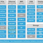
    Moore’s is still the law, and device scaling remains the key focus of front-end process research, however next-generation technologies–and the Big Data, cloud computing world that supports mobile, IoT, and other next-gen applications–are the new drivers, bringing new demands and challenges running parallel with Moore’s Law.

    450mm, EUV, and 3D IC may have hit bumps on the road to the future, but their progress still drives the discussion and the debate over what comes next for the microelectronics industry.

    Advanced Device Manufacturing Drives the Discussion at SEMICON West 2014

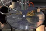
    SEMICON West is the flagship annual event for the global microelectronics industry. It is the premier event for the display of new products and technologies for microelectronics design and manufacturing, featuring technologies from across the microelectronics supply chain, from electronic design automation, to device fabrication (wafer processing), to final manufacturing (assembly, packaging, and test). More than semiconductors, SEMICON West is also showcase for emerging markets and technologies born from the microelectronics industry, including micro-electromechanical systems (MEMS), photovoltaics (PV), flexible electronics and displays, nano-electronics, solid state lighting (LEDs), and related technologies.


    Add a paid program and get your exhibits pass FREE!
    Add just one paid program to your SEMICON West registration and your exhibits pass is FREE! That’s a savings of $150 onsite–PLUS Early Bird pricing on programs is good through June 6, saving you even more! Register now!

    Paid SEMI Technology Symposium (STS) packages include premium content, guaranteed seating, and networking lunches!

    Device Manufacturing/Wafer Processing Highlights at SEMICON West 2014

    [TABLE] style=”width: 430px”
    |-
    | colspan=”2″ align=”left” valign=”top” style=”width: 430px” | Tuesday, July 8, 2014
    |-
    | colspan=”2″ align=”left” valign=”top” style=”width: 430px” |
    |-
    | align=”left” valign=”top” style=”width: 150px” | 9:00am-12:00pm
    | align=”left” valign=”top” style=”width: 280px” | STS Session: Challenges, Innovations and Drivers in Metrology
    Session Partner: SEMATECH
    Moscone North, Hall E, Room 130
    Paid session

    |-
    | colspan=”2″ align=”left” valign=”top” width=”430″ |
    |-
    | align=”left” valign=”top” width=”150″ | 1:30pm-4:30pm
    | align=”left” valign=”top” width=”280″ | Yield Session: Defectivity and Process Variability, Inspection, Defect Reduction Challenges and Process Controls at the Sub 20nm Nodes
    Session Partner: SEMATECH
    Moscone North, Hall E, Room 130
    Paid session

    |-
    | colspan=”2″ align=”left” valign=”top” width=”430″ |
    |-
    | align=”left” valign=”top” width=”150″ | 1:30pm-3:30pm
    | align=”left” valign=”top” width=”280″ | Variability Control – A Key Challenge and Opportunity for Driving Towards Manufacturing Excellence
    TechXPOT South, South Hall
    Free session

    |-
    | colspan=”2″ align=”left” valign=”top” width=”430″ |
    |-
    | colspan=”2″ align=”left” valign=”top” width=”430″ | Wednesday, July 9, 2014
    |-
    | colspan=”2″ align=”left” valign=”top” width=”430″ |
    |-
    | align=”left” valign=”top” width=”150″ | 9:00am-12:00pm
    | align=”left” valign=”top” width=”280″ | Getting to 5nm Devices: Evolutionary Scaling to Disruptive Scaling and Beyond
    Moscone North, Hall E, Room 131
    Paid session

    |-
    | colspan=”2″ align=”left” valign=”top” width=”430″ |
    |-
    | align=”left” valign=”top” width=”150″ | 10:30am-12:30pm
    | align=”left” valign=”top” width=”280″ | Subcomponent Supply Chain Challenges for 10 nm and Beyond
    Hosted by: SEMI Semiconductor Components, Instruments, and Subsystems Special Interest Group
    TechXPOT South, South Hall
    Free session

    |-
    | colspan=”2″ align=”left” valign=”top” width=”430″ |
    |-
    | align=”left” valign=”top” width=”150″ | 1:30pm-4:30pm
    | align=”left” valign=”top” width=”280″ | Readiness of Advanced Lithography Technologies for High-Volume Manufacturing
    Moscone North, Hall E, Room 131
    Paid session

    |-
    | colspan=”2″ align=”left” valign=”top” width=”430″ |
    |-
    | align=”left” valign=”top” width=”150″ | 1:30pm-3:30pm
    | align=”left” valign=”top” width=”280″ | Productivity Solutions for 300mm and Smaller
    Hosted by the Secondary Equipment and Applications Americas Chapter
    TechXPOT South, South Hall
    Free session

    |-
    | colspan=”2″ align=”left” valign=”top” width=”430″ |
    |-
    | colspan=”2″ align=”left” valign=”top” width=”430″ | Thursday, July 10, 2014
    |-
    | colspan=”2″ align=”left” valign=”top” width=”430″ |
    |-
    | align=”left” valign=”top” width=”150″ | 9:00am-12:00pm
    | align=”left” valign=”top” width=”280″ | STS Session: 450mm Technology Development Update
    Moscone North, Hall E, Room 131
    Paid session

    |-
    | colspan=”2″ align=”left” valign=”top” width=”430″ |
    |-
    | align=”left” valign=”top” width=”150″ | 1:30pm-3:30pm
    | align=”left” valign=”top” width=”280″ | STS Session: Breakthrough High Volume Manufacturing Innovations: New paradigms for the Road Ahead
    Moscone North, Hall E, Room 131
    Paid session

    |-

    Register now and save! Early Bird pricing ends June 6

    SEMICON West 2014
    Exhibits: July 8-10
    Programs: July 7-11
    Moscone Center
    San Francisco, CA
    www.semiconwest.org
    #semiconwest

    Other SEMI Events

    SEMI Member Day (Aurora, IL) — May 29
    An exclusive SEMI member event in the North Central region.

    Northeast Tech Talk (Billerica, MA) — June 25
    From Paper to e-Paper; How E ink Display Technology is Changing the World

    Strategic Materials Conference (SMC 2014) — September 30-October 1
    Materials Matter–Enabling the Future of IC Fabrication and Packaging

    International Technology Partners Conference — November 9-12
    New Structures for Innovation

    Industry Strategy Symposium – ISS 2015 (Half Moon Bay, CA) — January 11-14
    “Riding the Wave of Silicon Magic”

    lang: en_US


    Motley Fools Intel Investors Again!

    Motley Fools Intel Investors Again!
    by Daniel Nenni on 05-22-2014 at 12:00 pm

    It really is quite a racket. Investor bloggers spread semiconductor disinformation for $.01 per click, that coincidentally covers their stock positions, and I get paid $300 per hour to explain it to Wall Street. While I appreciate the opportunity to bond with the financial people, I do wonder how these bloggers sleep at night.

    Here is the latest disinformation from Motley Fool:

    While Taiwan Semiconductor (NYSE: TSM ) , Samsung (NASDAQOTH: SSNLF ) , and others have been claiming that everything is going swimmingly for production during 2014, the reality from the semiconductor equipment vendors’ point of view is a different one that should allow Intel (NASDAQ: INTC ) investors to breathe a sigh of relief.

    My translation: Please don’t sell your Intel stock until I cover my position. The reality from the semiconductor equipment vendors is that they will miss Wall Street’s expectations so it’s finger pointing time. Just once I would like to hear a CEO on a conference call say, ”You know what, we screwed up, it’s all our fault, we deserve a stock downgrade.”

    In short, while TSMC and Samsung talk a big game with respect to their FinFET nodes, the truth is that the foundries are having a difficult time getting the yields to be passable and seem to be quite a way from production. The question, then, is how far from volume production are the foundries?

    Wait, did he just call TSMC and Samsung liars? At the 25[SUP]th[/SUP] Annual TSMC Technology Symposium last month customers (close to 1k people I would guess) got a complete update:

    TSMC Updates: 20nm, 16nm, and 10nm!

    Unfortunately or fortunately only semiconductor professionals were invited so the investor bloggers don’t know any better.

    By the way, this particular investor blogger also published this:

    Intel’s 14 Nanometer: It’s Here And It Kicks ButtSeptember 15, 2013
    At the very first keynote by new Intel (INTC) CEO Brian Krzanich, I had a front row seat to the demonstration of the world’s very first, fully-working 14 nanometer microprocessor. Folks, this isn’t some “test chip”, but a bonafide, fully-functional, Windows-booting microprocessor that is set to go into production by Q4 2013.

    Paul McLellan and I sat in the 5[SUP]th[/SUP] row and having published earlier that Intel 14nm would be delayed we were quite shocked. SemiWiki readers know the rest of this story, Brian K. had to eat crow in his next conference call and admit that 14nm would in fact be delayed. The 14nm microprocessor mentioned above is now set to hit shelves by Q4 2014.

    So the truth is that Intel was having a difficult time getting the yields to be passable and seem to be quite a way from production.

    As I mentioned before, disinformation is a competitive weapon and something publicly traded companies are good at. Most of these investor bloggers are spoon fed PR stuff, they cut and paste the rest to support what’s in the spoon. Add in the personal bias of owning the stock and you get a serious amount of disinformation, which is why Wall Street keeps calling.

    Just my opinion of course! :rolleyes:

    More Articles by Daniel Nenni…..

    lang: en_US


    Variation-Aware Custom IC Design Best Practices

    Variation-Aware Custom IC Design Best Practices
    by Daniel Nenni on 05-21-2014 at 1:00 pm

    I’ve worked with Solido for 5 years, and it’s been a pleasure to watch the world’s top semiconductor companies and foundries adopt Solido software for their SPICE simulation flows.

    Sub-28nm design starts are accelerating, growing from 150 in 2012 to 900 this year. The move to sub-28nm design nodes is being driven by consumer electronic demands to improve speed, connectivity, reliability, battery life, form factor and cost. For example, according to TSMC data, TSMC 16nm FinFETs versus TSMC 28nm gets 2X gate density, 38% speed improvement at same power, and 54% improved power savings at the same speed.

    According to ITRS, threshold voltage variation has increased from 25% in 2005 to 58% in 2013. Threshold voltage variation sources in FinFET transistors are gate length, fin thickness, oxide thickness, random dopant fluctuations, oxide charge and work function. Foundries like TSMC, GlobalFoundries, Samsung and Intel are now providing detailed statistical models in their PDK’s that characterise local (mismatch) and global manufacturing variation data so that designers can get working silicon at suitable yields without having to over-design, taking power, performance and area hits. Since sub-28nm design and implementation cost is more than $100 million, a single design respin can cost over $10 million plus the lost time-to-market product revenue.

    The required number of SPICE simulations have increased 10X to 1,000,000X to get the needed design coverage using the advanced node PDK’s, making variation-aware custom IC design tools a standard part of the design flow. While SPICE simulators are focused on fast, accurate and high-capacity simulation, variation-aware custom IC design tools are complementary providing SPICE simulator control and analytics. This enables users to improve design coverage with orders-of-magnitude fewer simulations than brute force for PVT corner analysis, 3-sigma Monte Carlo design and 4- to high-sigma Monte Carlo design. As a result, SPICE simulators together with variation tools are being used in the SPICE simulation flow at advanced nodes.

    There is a panel on Variation-Aware Custom IC Design Best Practices at the Design Automation Conference this year. The panel discussion will focus on best practices and methodologies for variation-aware memory, standard cell, analog/RF, and custom digital design. Panel topics will span 4- to high-sigma Monte Carlo verification, high-sigma cell optimization, 3-sigma Monte Carlo verification, verification across 100,000+ PVT/parasitic corners and statistical PVT corners, FinFET variation, variation debug, analog calibration/trimming and SPICE simulation requirements for variation analysis.

    Panelists will be Mark Erikson from Broadcom, Jaeha Kim from Seoul National University, Irina Ilatov from Sidense and Trent McConaghy from Solido Design Automation. The panelists have extensive experience developing and deploying variation-aware methodologies in their companies, which should make this an interesting and informative session.
    The panel is on DAC Monday and is free to attend. Register for the panel here: https://www.surveymonkey.com/s/6N5LTNC

    Panel attendees will be given a complimentary copy of the book written by Paul McLellan and I called Fabless: The Transformation of the Semiconductor Industry.

    You can also register for a suite demonstration of Solido Variation Designer software here: http://www.solidodesign.com/page/dac-2014-demo-signup/

    More Articles by Daniel Nenni…..

    lang: en_US