There are too many IoT protocols. Way too many. Anyone who says one single protocol will be the winner from end-to-end in all IoT applications and markets is smoking something. Software defined, multi-protocol gateways are the only hope on the IoT – and DSP cores enable this strategy. Continue reading “Winning the IoT protocol battle with DSP”

Jean-Louis Gassée on Intel and Mobile
I came across a very interesting article/blog written over the weekend by Jean-Louis Gassée on Intel and mobile. It covers some similar ground to several of my blog posts on the topic but also has some new facts. And it has additional credibility since Jean-Louis was head of product development and worldwide marketing at Apple (pre-iPhone).
He also refers to an interviewfrom last year that I hadn’t read with Paul Otellini, Intel’s then-CEO on his last day. Apparently Jobs gave Intel the chance to build the processor for the first (and so presumably subsequent) iPhones. Intel turned them down. Otellini said:We ended up not winning it or passing on it, depending on how you want to view it. And the world would have been a lot different if we’d done it. The thing you have to remember is that this was before the iPhone was introduced and no one knew what the iPhone would do. At the end of the day, there was a chip that they were interested in that they wanted to pay a certain price for and not a nickel more and that price was below our forecasted cost. I couldn’t see it. It wasn’t one of these things you can make up on volume. And in hindsight, the forecasted cost was wrong and the volume was 100x what anyone thought.
That was the day Intel failed in mobile. This would have been an ARM-based chip. But at the time Intel had an ARM-based division called Xscale (the old Digital StrongARM) who were desperate for business. Eventually they sold off the whole division to Marvell in 2006.
When I was at VLSI I worked for a guy called Cliff Roe who said “I wouldn’t want to be Intel’s next CEO [this was in the Andy Grove era]. He has to find a way to educate the company and Wall Street that they can’t go on making those kind of margins.” Well they still have those kind of margins (Intel’s gross margin is an astounding 65%). But it is also a genuine problem. If Intel had won Apple’s business they would now be building about 250M application processors per year at a cost of, say, $20-40 which is a $5-10B business, significant given Intel’s total business is around $60B. But it would be at a much lower margin since the ARM market is competitive and the x86 market is not (AMD is the only competitor and not a strong one). Whether Wall Street would treat this as good or bad is unclear. They love Intel’s margins.
Intel’s entire strategy has been that they are 3 years ahead of everyone else in manufacturing and process. Indeed they highlighted this at their recent analyst day. The chart is also a bit self-serving. Intel introduced FinFET at 22nm, compared to TSMC at 16nm. But TSMC introduced double patterning at 20nm compared to Intel at 14nm. I have no insight into whether Intel’s 14nm yield problems have anything to do with double-patterning learning ramp, but it is certainly the biggest different from 22nm.
But they need to ship $50 of negative revenue with each tablet processor because they are so competitive! And even in their main business a lot of Broadwell is being pushed out to the middle of next year. I think what actually happens is that Intel has a process lead but only for microprocessors where their price is so high that they don’t need the process to be truly competitive. Everything else has to run in old processes making them non-competitive too.
Herethey were in 2012:Intel dismisses ‘x86 tax’, sees no future for ARM or any of its competitors
How’s that going a couple of years later? ARM is still solidly entrenched in mobile and the rumors that Apple will switch their MacBook Air and maybe Pro to ARM are getting stronger.
Now Intel will roll mobile in with the non-server processors so the fact that they are currently losing $1B per quarter on it (perhaps $7B over the last two years) will be be hidden from view. Or maybe they are quietly giving up, who knows?
But the next big thing is Internet of Things (IoT) and that is a perfect market for Intel with lots of differentiation, because…nobody has a clue. And margins in IoT are likely to be even lower than mobile and ASPs lower still (these will not be mammoth chips in 10nm). I believe most IoT devices will be build on older nodes so whether Intel is 3 years ahead or not is irrelevant.
See also Intel Quits Mobile
See also Intel is Not Quitting Mobile
See also Intel Quarterly Results
NoC IP boosts SoC reliability, fault tolerance
System-on-chip (SoC) devices are increasingly becoming more complex in terms of adding functionality yet they need to be more reliable and fault tolerant for automotive, aerospace and industrial electronics.
Arteris Inc.—which invented the network-on-chip (NoC) interconnect technology back in 2006—is now offering FlexNoC Resilience Package to allow SoC designers augment network-on-chip interconnect IP to boost safety and reliability in mission-critical electronics.
“It is part of the computational consolidation of the multicore SoC designs as CPU-only safety mechanisms like ECC and dual-core lockstep (DCLS) are not sufficient for automotive, aerospace, defense, industrial equipment and other electronics markets requiring fault tolerance,” said Kurt Shuler, VP of Marketing at Arteris. “The network-on-chip interconnect IP solutions like FlexNoC can serve as the central nervous system of an SoC with 150-200 blocks of communication.”
The SoC devices for safety-related applications in the automotive, industrial and medical markets usually use ARM Cortex-R5 and Cortex-R7 processors. These CPU core IPs implement techniques like ECC, parity data protection, DCLS redundancy, duplicate internal memories, safety checkers, and built-in self-test (BIST).
The CPU-only approach, however, falls short in providing the end-to-end protection of any or all IP-to-IP communication within the SoC. That’s where the resilience features for on-chip interconnect—like FlexNoc—come into play and provide support for ARM Cortex-R5 and Cortex-R7 processors port checking.
The FlexNoC Resilience Package enables the implementation of data protection and control features, and it doesn’t require the replacement of existing fabric IP or tools. The easy partitioning of SoCs means that IC designers can take an existing chip and specify which parts of an SoC require resilience and which do not.
FlexNoC Resilience Package block diagram
What is resilience? It’s the ability to maintain an acceptable level of service in the face of faults and challenges to normal operation. Digital ICs can fail in many ways. There could be glitches in power supply or clock supply leading to transient electrical problems, or there could be soft errors or physical damage.
How network-on-chip works
Tom Hackenberg, Principal Analyst, Automotive Embedded Processors, IHS Technology Inc., said: “A growing number of chipmakers are turning to safety and security optimized network-on-chip subsystems for SoCs, such as FlexNoC Resilience Package, to lower the development costs and time it takes to achieve the ISO 26262 certification, enabling both media-intense processing and certifiable mission-critical solutions in an integrated SoC.”
Take the automotive industry as a case study. Automotive OEMs are using high-performance SoC solutions common to the wireless market amid the growing demand for media-rich and telematics applications. However, they have to merge these SoC solutions with time-consuming and intense MCUs and CPUs that are ISO 26262 and ASIL certified, so that these SoCs can provide safe and reliable control systems. According to Hackenberg, while it’s common to design separate electronic control units, it can increase the cost and potentially add to driver distraction.
That’s where network-on-chip subsystems for SoCs come into the picture as a valuable piece of technology. The network-on-chip IP solutions like FlexNoC Resilience Package protect safety-critical portions of the entire CPU, SoC interconnect and memory path, and thus help OEMs create more reliable and fault tolerant systems in shorter time and with lower cost. Semiconductor vendors like Altera and Renesas have been using FlexNoC Resilience Package to make their SoC designs faster and more dependable.
More product details are available in the technical paper, “SoC Reliability Features in the FlexNoC Resilience Package.”
Image credit: Arteris Inc.
Majeed Ahmad is author of Age of Mobile Data: The Wireless Journey To All Data 4G Networks that chronicles the evolution of mobile data technology and how that eventually led to pure data LTE network architecture.
A Closer Look at the QCOM $40M Investment in China!
Last Thursday night was the 20[SUP]th[/SUP] annual GSA Awards Dinner which probably hosts one of the largest collections of semiconductor executives. Think of a movie or music awards show with all of the trimmings including Jay Leno as the keynote. I don’t know the exact head count but there were 160 dinner tables with 10 plates per table. The GSA (Global Semiconductor Association) used to be called the FSA (Fabless Semiconductor Association) which means the IDMs can play with us too but it was mostly fabless.
About GSA:
The Global Semiconductor Alliance (GSA) mission is to accelerate the growth and increase the return on invested capital of the global semiconductor industry by fostering a more effective ecosystem through collaboration, integration and innovation. It addresses the challenges within the supply chain including IP, EDA/design, wafer manufacturing, test and packaging to enable industry-wide solutions. Providing a platform for meaningful global collaboration, the Alliance identifies and articulates market opportunities, encourages and supports entrepreneurship, and provides members with comprehensive and unique market intelligence. Members include companies throughout the supply chain representing 30 countries across the globe. www.gsaglobal.org
Earlier in the day Qualcomm announced the China investment with Walden International which is interesting because the CEO of QCOM (Steve Mollenkopf) and the founder of Walden International (Lip-Bu Tan) were both there last night and very friendly. Even more interesting, the founder of Walden International is also the CEO of Cadence and QCOM is a very big customer of Cadence. ARM and TSMC are also investors in Walden and both of their CEOs were there as well. Cadence is also very active with ARM and TSMC (I see Lip-Bu in Taiwan the more than any other EDA CEO) so it is indeed a very small pond we swim in. Given that China consumes roughly half of the semiconductors we produce I think you will see more of these types of deals amongst “fabless friends”, absolutely.
Qualcomm Ventures, the investment arm of Qualcomm, was formalized in 2000 and currently has a portfolio of more than 120 active companies across the globe. Qualcomm Ventures also invests in seed stage companies through its QPrize” Mobile Internet Startup Competition which evaluates and awards seed funding for promising early stage Chinese entrepreneurs.
If you look at their portfolio page you will see some very interesting and innovative companies that no doubt integrate QCOM technology (FitBit, Xiaomi). If you hover over the 100+ logos you will see the future of mobile and IoT especially in India and China.
Dr. Morris Chang Exemplary Leadership Award
The Dr. Morris Chang Exemplary Leadership Award recognizes individuals, such as its namesake, Dr. Morris Chang, for their exceptional contributions to drive the development, innovation, growth and long-term opportunities for the semiconductor industry.
- 2013 Dr. Sehat Sutardja, Chairman, CEO and Co-Founder and Ms. Weili Dai, President and Co-Founder, Marvell Technology Group Ltd. (Marvell)
- 2012 Sir Robin Saxby, Founding CEO, ARM
- 2011 Dr. Henry Samueli, Co-founder and Chief Technology Officer, Broadcom Corporation
- 2010 Dr. John Hennessy, president of Stanford University
- 2009 Dr. Aart de Geus, Chairman & Chief Executive Officer, Synopsys, Inc.
- 2008 Dr. Eli Harari, Chairman and CEO, SanDisk Corporation
- 2007 Gordon Campbell, Executive Director, TechFarm Ventures
- 2006 Kamran Elahian, Chairman, Global Catalyst Partners
- 2004 Jen-Hsun Huang, CEO, President and Co-Founder, NVIDIA Corporation
- 2003 Dr. Irwin Mark Jacobs, Chairman of the Board and Chief Executive Officer of QUALCOMM Incorporated
- 2002 Bernard V. Vonderschmitt, Co-Founder and Chairman of the Board, Xilinx, Inc.
- 2001 Michael L. Hackworth, Chairman of Cirrus Logic
- 2000 Dr. Robert S. Pepper, former President and CEO, Level One Communications
- 1999 Dr. Morris Chang, Chairman and CEO, TSMC
The most interesting award given out last night was the Dr. Morris Chang Exemplary Leadership Award. Interesting because it went to Dr. Morris Chang for the second time (Dr. Mark Lui accepted for Morris). This will probably keep the semiconductor rumor mill churning for a while and you read it here first!
Also Read: Fab-U-Less! The 2013 Global Semiconductor Awards!
Virtual Emulation Extends Debugging Over Physical

Amid burgeoning complexity of SoC verification with ever increasing hardware, software and firmware content, verification engineers are hard pressed with learning multiple tools, technologies and methodologies and still completing SoC verification with full accuracy in time. The complexity, size and diversity of SoC has increased while time-to-market has decreased, thus compressing the time to design and verify. The engineering team scattered across the globe need access to limited common verification resources, especially hardware emulators in order to gain confidence in complete SoC verification. Emulators are generally stored in labs and are accessed physically, thus limiting their access to a larger team. What if the emulator environment is virtualized and is made available to the verification team across the globe? It will unleash the resource capability, scale up verification and improve design and verification team productivity by large extent.
Lauterbach’shardware assisted debug toolset TRACE32 and Mentor’sVeloce emulator provide a unified debugging environment that can be used in virtual (for models and simulators) as well as physical (for FPGA prototypes and silicon) mode.
Veloce OS3 emulation system provides a complete verification environment (integrated with Questa simulation environment) for software and hardware engineers through a unique architecture that enables simulation-like interactive debug and fast turnaround for SoC configurations that can scale up to 2 billion gates. It’s standards compliant (SCE-MI 2) providing interoperability with other software-based hardware simulators. Providing visibility of all nodes at all times, it can be used for pre- as well as post- silicon debug.
Through VirtuaLAB environment, multiple users across the globe can simultaneously run verification remotely on the same machine. The Veloce OS3 VirtuaLAB peripherals are reconfigured instantly to support multiple projects and rapidly shifting priorities. This enables global emulation resource management which maximizes engineer productivity and verification ROI. The verification environment is flexible enough to allow hardware stimulus through physical connection, software stimulus through virtual connection, or a combination of the two.
In physical connection, the difference in voltage levels and speeds between actual silicon and Veloce emulation model is solved by Veloce iSolve products (that includes iSolve ARM Cortex JTAG Trace) through a range of solutions including Ethernet, USB, multimedia, and debug.
Veloce offers a co-modelling environment where a user can use virtual environments (e.g. C models) in a host computer connected to the actual hardware design (RTL) implemented in Veloce. This approach can be used to replace hardware solutions (e.g. physical debug probe) with a software model, thus enabling concurrent users to access a single build of design. In the above diagram, untimed transactions are being transferred over TBX (Veloce TestBench Xpress) link to Veloce with the vJTAG transactor translating these into a stream of JTAG pin level transitions. This improves performance compared to co-simulation environment which transfers the individual JTAG pin level transitions over the TBX link.
Veloce iSolve allows users to connect the real debug hardware used on a FPGA prototype or silicon platform. Virtual Probe replaces the physical solution, enabling a virtual connection of the JTAG debugger to the design through the TBX co-modelling interface. Both iSolve and Virtual Probe support the same debugger UI environment.
A Virtual Probe is implemented within the co-model host using both Lauterbach and Mentor software. The T32MCIServer replaces the debug hardware; the vJTAG transactor interface takes the JTAG sequence transactions from the T32MCIServer and sends them over TBX to the Veloce which recreates IO pin signals at the SoC boundary.
TRACE32 contains a debug probe, a real-time trace tool, and a logic analyzer which are architecture independent and can be operated either standalone or integrated together through a system controller. It supports all common microprocessor architectures in the embedded world.
A detailed description about connecting TRACE32 and iSolve ARM Cortex JTAG Trace as well as connecting TRACE32 and Virtual Probe along with other details about this methodology is provided in a whitepaperat Mentor website.
Both, the physical and virtual methods have distinct advantages; the physical connection for final testing of a design before tape-out provides a very high level of confidence that the real hardware after manufacturing will work with the real debugger; the virtual connection provides highly flexible enterprise level solution for multiple concurrent remote users to develop software and testbenches that use TBX.
Will 3DIC Ever Be Cheap Enough for High Volume Products?
More news from the 3DASIP conference. Chet Palesko of SavanSys Solution had an interesting presentation with the same title as this blog (although this blog draws from several other presentations too). Chet took a look at what aspects of 3D are likely to get cheaper going forward. He took as a starting point that stuff that is not used only for 3D is probably already close to as cheap as it is going to be. For example, 3D chips involve bumping as does flip-chip. So although there may be some small amount of incremental improvement in cost, most of the improvement has already happened driven by flip chip. And, as an interesting aside, flip chip is still more expensive than wire-bond which is why it is only used for about 17% of chips. You only use flip chip if you need it for other reasons than cost (smaller package, higher performance etc).
Another thing that I had not thought of is that 2.5D is expensive compared to true 3D. Of course you have to manufacture the interposer, which is done in a non leading edge process such as 65nm. But the TSV and bumping it requires is very costly since it is large so not many interposers-per-wafer. There are some savings since the die don’t need TSVs, but they still all need bumping. Qualcomm, in particular, maintain that interposers are the wrong way to go (not that they have any 3D chips in production though). At a conference in Europe recently someone had numbers showing 2.5D was 6 times the cost of true 3D although that seems high to me (but I’ve not seen those numbers).
So 3DIC is only the best choice if no other technology meets the product requirements, typically things like memory bandwidth, physical package size, ultra low power and so on. Most technologies are ones of last resort in that they are more expensive but have other advantages (embedded passives, multi-chip modules, even SoCs). A few are cheaper and thus displace the existing technology. Surface mount displaces through-hole assembly, until recently, each new process node displaced the previous one (at least for digital logic).
Earlier Jan Vardarman had listed out the big pictures areas where improvement are needed:
- EDA tool availability (especially pathfinding and thermal analysis)
- Assembly: stacking of die
- Wafer thinning and the temporary attach and debond process
- Thermal, especially logic on memory (since hot spots may take DRAM out of spec)
- Test methodology and the need for known-good-die (KGD) making wafer sort so much more important and costly
- Yield of the whole process
- Setting up the whole supply chain and who does what
To keep it simple, let’s assume a 3DIC with just two die, a bottom die and a top die. The bottom die cost drivers are TSV creation, TSV reveal (basically CMP), TSV creation yield loss, thin wafer yield loss, testing/known-good-die costs.The top die cost drivers are the RDL process cost and the wafer bumping cost. Then assembling the two die has silicon to silicon process cost, silicon to silicon yield loss, silicon to substrate and substrate cost. So which of these will have big improvement potential? See the tables below. The column on the right summarizes whether improvement is likely. Click on the tables to enlarge them.
Chet looked at some alternatives but to wrap up he told us we were asking the wrong question. The right question is “Will the markets that require 3DIC grow fast enough to drive volume manufacturing?” After all, performance, power and miniaturization trends are continuing. And there will be some cost reduction for 3DIC which can open up new markets. One caveat is that the cost of 2.5D packaging (such as the Xilinx FPGA) should not be extrapolated to 3D. Even so, 3D is unlikely to ever be the cheapest solution and if you can package-on-package (like the Apple Ax chips) or fanout-wafer-level (FOWLP) you will.
But in the same way people design SoCs if they cannot use an FPGA or do a board-level design, people will use 3D when nothing else will do. Like the memory stacks announced by Micron, Samsung and SK-Hynix, the recently announced graphics integrations by Nvidia and AMD/ATI, the Xilinx high-end FPGAs and so on. These are all (or soon will be) in production but at comparatively low volumes.
Benefits of Using Schematic Driven Layout
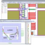
Most IC designs are developed by a team of professionals, often separated into distinct groups like front-end and back-end, logical and physical designers. Circuit designers use tools like schematic capture at the transistor-level to create a topology, then begin simulating the netlist with a SPICE simulator. Layout designers can manually place transistors, contacts, vias, cells and interconnect between cells. How should the circuit designers communicate their layout preferences to the layout designers?
A recommended approach is to use Schematic Driven Layout (SDL), a technique where on the front-end you can start to control where the initial placement of physical transistors and cells will happen, all without having to be an IC layout expert. Every schematic device gets a corresponding layout device, reducing the amount of time spent in LVS (Layout Versus Schematic). Time to market is the familiar driver in all electronics companies, so saving time by using an SDL flow can really help out.
There’s a webinaron this topic scheduled by Tanner EDA for Tuesday, December 16th at 11:00 AM Pacific time. Expect to learn the following concepts:
- Schematic Capture with the S-Edit tool
- Layout editing with the L-Edit tool
- Schematic Driven Layout (SDL) starting with S-Edit
- Using assisted routing in an SDL design flow
- Eliminating manual routing
- ECO tracking
Related – IC Place and Route for AMS Designs
Both circuit design engineers and layout designers would benefit from attending this SDL presentation. From past Tanner EDA webinars I know that the presenters use the EDA tools live, instead of just canned screen shots. Thuong U is the AE doing the presentation, and he has 13 years of experience with these EDA tools.
Related – Adding a Digital Block to an Analog Design
Manual routing is a technique often used in AMS designs in order to get tighter control over matched device requirements, however by adding assisted routing you can get results more quickly while maintaining the accuracy. Schematic Driven Layout isn’t just offered by the big three in EDA, so having this at Tanner EDA gives you some choice in buying tools for your next AMS project.
Webinar
Register for this free webinar online.
Related – Affordable AMS EDA Tools at DAC
3D, The State of the State
I have been at the 3D ASIP conference that is held every year in Burlingame. It is far and away the best place to get a snapshot on what is going on in 3D (and 2.5D) IC design each year. One of the presentations was by the guys from Yole on where the industry is right now. Other presentations were on pathfinding, power reduction (did you know Jerry Frenkil likes Lone Star Beer?), building TSVs, planarity during assembly and much more.
In the past the conference has been all about how 3D is going to happen “real soon now” but each time a 3D design was announced it would turn out that when the teardown was done it didn’t use thru silicon vias (TSVs) or any true 3D technology at all. It would be another year before something happened. But this year things started to happen.
3D and 2.5D are still too expensive for most applications, but the ones that can take advantage of the benefits and sell them to their customers are moving. Don’t expect 3D chips to show up in your cell-phone any time soon but in routers, and servers and high-end stuff it is starting to move. Samsung did a study that showed that compared to package on package designs (like the current Apple Ax designs) package size was down, power was down and bandwidth was up insanely. Designs where those are valued make sense.
There are some pretty high profile 3D things happening. The earliest was the Xilinx high end FPGA but that ships in very low volume at very high prices so isn’t really generating enough learning to get prices down. Samsung has announced DDR4 3D DRAM DIMM modules. The Micron hybrid memory cube is about to start shipping in volume: 4 memory chips on top of a logic chip with all the control logic. SK Hynix and Samsung have also announced 3D memory products moving into high volume manufacturing.
Announced, but not shipping are that AMD (ATI) will use 3D stacked high bandwidth memory (HBM) on 20nm in 2Q next year. Nvidia will do the same in 2016. Intel has said they have the technology but haven’t announced anything but then they are Intel. Even at the lower end of the market Matrox has announced next generation GPU modules powered by AMD 3D stacks. If you want to be in graphics, get with the program.
There are other designs too. The common characteristic is that they are at the high end of the market so that although 3D is still expensive, it has higher performance/bandwidth and for those markets that need it the ends justifies the cost. I have no idea of the cost of Micron’s HMC but they admit it is a lot more than just buying the same amount of regular DRAM. But the performance is so much higher that if you are building high end servers or routers then you can justify it.
The big driver in SoC these days is mobile, but it is too cost-sensitive so nobody seems to expect 3D to appear there any time soon. Qualcomm are on record of saying that the costs of interposers are too high for now and given all the growth in mobile is in the low end that you shouldn’t expect to see it any time soon.
For really big chips the savings from 2.5D can be big. A couple of years ago I was at a 3D workshop where eSlilicon ran their cost model on the Xilinx parts and reckoned they were saving 80% by doing a 2.5D interposer with 4 small chips versus trying to run a maximum (reticle limit) sized die on an immature process.
So 2015 is the year of 3D. It is coming. Yes, only in high priced products for now, but as the learning from running in volume starts to percolate through the supply chain it will get more economical. There don’t seem to be any major technical problems (we know how to build TSVs, even though they will get better; we know how to attach and debond a backing material so that when we thin the die it is manageable; the stress issues with different thermal expansions seem manageable). The big issues seem to be to run a lot of volume and to decide who does what in the supply-chain.
IoT is a 3D market. They are not going to go to 16nm. They need sensors, RF, analog and digital in the same package at cheap cost. 3D is clearly the way that will eventually get there. Not next year, but eventually.
A Functional Verification Framework Spanning Simulation to Emulation
Software engineers and firmware designers can find bugs, update their code and re-distribute to the users. In the consumer electronics world this means that my smart phone apps get updated, and my Android OS gets updated on a somewhat regular basis, however on the hardware side the design and verification of an SoC must be close to perfect, because there’s no easy way to do a field upgrade and the cost of a product recall can put your company out of business. Performing functional verification on an SoC is the focus of my blog today, and there are several tasks required during the verification process:
Verification Activities, source: Wilson Research Group and Mentor Graphics
Our semiconductor industry has created and adopted the UVM (Universal Verification Methodology) as a standardized approach that can improve electronic product quality during verification. A SystemVerilog simulator used during verification can run maybe 10-1,000 clock cycles per second, depending on the block size and at that speed it just isn’t fast enough to boot an operating system, or paint a screen with pixels.
Related – Coverage Driven Analog Verification
In typical fashion, where there’s a need, there’s often a product to meet that need, and for chip designers there are emulators which can run a few million clock cycles per second, allowing us to boot an operating system and fill a screen. The initial usage of UVM was focused on SystemVerilog simulators, so what about writing UVM testbenches that can also run on emulators?
Anoop Saha of Mentor Graphics wrote a detailed, 16 page white paper on this topic: From Simulation to Emulation – A Fully Reusable UVM Framework, and you may download it online. The idea is that verification engineers should be able to run tests in both a SystemVerilog simulator or emulator, support SystemVerilog in emulation, and provide faster test results in emulation than simulation.
To make your testbench compatible with an emulator use two components:
- An HDL (Hardware Description Language) static component with DUT (Device Under Test), which runs on the emulator
- The dynamic testbench running on the simulator, which contains the HVL (Hardware Verification Language) behavioral code
Here’s what these two blocks look like where yellow is the HVL, blue is the HDL, and green is the top-level:
Two top UVM Testbench
The interaction between HVL and HDL can further be refined by using a virtual interface construct where testbench components access SystemVerilog interfaces through a BFM (Bus Functional Model) interface. Shared parameters between HVL and HDL are defined in a common params_pkg file:
Acceleration ready two-top UVM architecture
The HVL code is strictly untimed in this approach because that would not work with emulation and slow down emulation. If you really need delays in a testbench then add them only inside of an HVL to HDL function call.
Related – Improving Verification by Combining Emulation with ABV
To keep the communication minimal between HVL and HDL we use a transaction level only, where testbench objects on the left-hand side use a virtual interface handle to access signals in the HDL on the right-hand side.
Communication between HVL and HDL
Testbench components on the HVL side can:
- Call tasks and functions inside the BFMs
- Drive and sample DUT signals
- Start BFM threads
- Configure BFM parameters
- Read BFM status
Virtual interface connection between HVL and HDL
Transaction-level modeling allows communication in both directions between HVL and HDL:
Inbound and Outbound Communication
Make sure that all of your function arguments are synthesizable to enable this two-way communication.
Transaction objects can use dynamic arrays or queues, so that you can model activity like Ethernet transactions. Streaming communication is accomplished through SCE-MI (Standard Co-Emulation Modeling Interface) pipes, where receiving and sending are running independent threads. Here’s an example of a SCE-MI pipe operation where the HVL sends a whole packet, then the HDL receives that across multiple clock cycles.
SCE-MI Pipes example
It is now possible to reuse a UVM testbench across both simulation and emulation by following the methodology of:
- Creating an untimed HVL testbench, and a timed HDL with the DUT and BFM logic
- The untimed HVL code has no delays
- HDL code must be synthesizable as defined by the emulator platform
- Remote function calls are used to communicate between HVL and HDL, no direct HDL signals called from any HVL class
Emulation is attractive because of its high speed, providing speed improvements over pure simulation by 50 to 5,000X. By using this approach you gain the verification benefits of using an emulator in simulation acceleration mode:
- Includes assertions
- Functional coverage
- Power aware
- Replay-based debug
- Reporting
- Profiling
The complete 16 page white paper, including coding examples is online now.
IDT bolsters RF portfolio amid LTE boom
The global rollout of fourth-generation wireless (4G) infrastructure requires new architectural frameworks for RF devices with demands like high linearity. Integrated Device Technology (IDT) Inc. is confident that its high-performance RF solutions for high-bandwidth communications will open a new window of opportunity in the continuing evolution of Long Term Evolution (LTE) technology.
The base station hardware now represents almost 50 percent of the wireless infrastructure market. And according to Earl Lum, President of EJL Wireless Research, LTE technology could comprise 90 percent of all RF base station system shipments by 2018.
According to Greg Waters, IDT’s President and CEO, the wired and wireless communications infrastructure business now represents two-third of IDT’s revenue. He particularly mentioned RF business tied to the burgeoning LTE networks as an exciting opportunity. “Fourth-generation base station manufacturers make up around US$50 to US$70 billion business,” Waters said. “At the same time, however, RF components in the 4G base stations need higher precision because of size and power constraints.”
Base stations traditionally generate a lot of power, but that has to change because the size of base stations is shrinking in the LTE-centric 4G networks. Another crucial challenge is the co-existence of 2G, 3G and 4G signals within the same spectral band. It is now imperative for base stations in the 4G environment to scale from macros to small cells while they improve in reliability as well as data throughput.
RapidIO is used in 100 percent of 4G rollouts
Here, Waters said, IDT’s expertise in RapidIO backplane communications will be highly valuable in reducing the overall network latency. “New LTE-Advanced and C-RAN designs are now adopting the RapidIO interconnect standard and it’s being used 100 percent in 4G rollouts.” Another prominent advantage that IDT claims to bring to its RF is expertise in signal integrity. “Signals from prepaid 2G users interfere with 3G and 4G users and that degrades quality of service (QoS) for the high ARPU business,” he added. “IDT’s expertise in signal integrity is critical in countering noise and interference.”
RF switch launch
IDT’s RF product portfolio includes mixers, digital step attenuators, modulators/demodulators and RF timing that encompass the design footprint from antenna to data converters. The San Jose, California–based chipmaker says it has over 40 RF products in production or sampling. IDT also claims to have captured 50 percent RF market share in China’s 4G network build-out.
The RF chips now represent the company’s fastest growing business. “We started from zero only five short years ago,” said Dave Shepard, VP and General Manager of IDT’s RF & Timing Division. “We are expanding our RF operations by 50 percent over the next 15 months.”
IDT has recently made an entry into the RF switch market with the launch of the F2912 device that offers low insertion loss and high isolation and linearity. It is aimed at 2G, 3G and 4G base stations, microwave backhaul and front haul, test equipment, CATV head-end, WiMAX radios, and general switching applications.
IDT’s F2912 RF switch
The F2912 chip supports the frequency range of 300 KHz to 8 GHz in order to achieve broad bandwidth without sacrificing performance across the entire frequency range. It boasts high isolation of 60 dB at 2 GHz to reduce signal leakage between adjacent RF port paths. It also features high OIP3 of +64 dBm to reduce intermodulation distortion. Moreover, the F2912 RF switch offers operating temperature range of -55 to 125°C for high reliability in harsh thermal environments.
More product details about the F2912 RF switch are available at http://bit.ly/1IiF9y3
Image credit: IDT Inc.
Majeed Ahmad is author of Age of Mobile Data: The Wireless Journey To All Data 4G Networks that chronicles the evolution of mobile data technology and how that eventually led to pure data LTE network architecture.