webinar IPXACT banner

Faster ECOs Using Formal Analysis

Faster ECOs Using Formal Analysis
by Daniel Payne on 02-28-2015 at 7:00 am

Your latest SoC has just begun the tape-out process and then marketing comes back with a small update to the specification to make your design more competitive, or maybe your regression tests just found a minor bug in a single IP block that needs to be fixed. Should you go back in your design flow, change the RTL source code and then completely re-run all of the logic synthesis and physical implementation tools? Probably not, instead you likely will opt for an ECO (Engineering Change Order) flow instead to save time. Since an ECO flow is often equated with manually editing a gate-level netlist and hacking together script files, there is plenty of room for introducing new errors into a design, so be careful.

Engineers at Synopsys have come up with a method to speed up this ECO process and at the same time add some automation to ensure that you’re not introducing any new bugs. I spoke by phone with Graham Etchells and Mark Patton to get an update on their Formality Ultra flow to manage and automate the ECO flow. Here’s the concept:


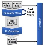
Functional ECO Implementation

A design change comes in, the design engineer updates the RTL code, Formality Ultra shows you exactly where in your gate level netlist the effected net is, and the ECO scrips are generated for both Design Compiler (logic synthesis) and IC Compiler (place and route) tools. There’s a final verification that the new netlist matches the changed RTL code.

Related – Formality Ultra, Streamline your ECOs

A manual ECO approach would have you looking at your gate-level netlist with a text editor after logic synthesis, trying to find a net of interest, after all of the optimizations and you may not even find your net name. With this automated ECO approach you can visually find your net of interest at the RTL or gate level, click on it, then see where this same net is in the post-synthesis netlist:


​Highlight equivalent nets

You can now implement and view each ECO interactively by:

  • Graphically using the Verdi nECO tool

or

  • With macro commands

ECO Schematic Editing

There’s even a way to see where your changed nets are in both the RTL and layout views, helping you to understand the physical impact before committing to a change.


Cross-highlightint

Verification of each ECO now only takes minutes, because only the limited areas of the logic change are automatically identified and run. Even if your entire design is millions of gates, the ECO verification runs in minutes so you can do more what-if analysis on how to best implement each ECO.

Related – LSI’s Experience with Formality Ultra

Once you are satisfied with each ECO fix, then the scripts to control IC Compiler and Design Compiler are created automatically:


Integrated Tool Flow

Most ECO changes effect a few dozen gates, so if your RTL changes impact hundreds of gates or more then you’ll probably just re-synthesize and re-implement that part of your design instead of trying an ECO flow.

Related – How STMicroelectronics uses Formal Tools (Webinar)

Summary

SoC designers can be more productive by moving from a manual ECO flow to a more automated approach using the Formality Ultra, Design Compiler and IC Compiler flow. Instead of taking weeks on a manual ECO approach, you can now do the same work in days. The learning curve for Formality Ultra is a day or two, and customers like Cavium and Centaur Technology are shaving valuable time off their schedules.


Mentor 2014 Results

Mentor 2014 Results
by Paul McLellan on 02-27-2015 at 7:25 pm

Yesterday Mentor announced their quarterly results. Since their financial year is not aligned with the calendar year, this was also the end of their fiscal 2015. The quarter was an all-time record with revenues of $439M and (non-GAAP) EPS of $1.09. The year was also an all-time record with revenues of $1.24B and EPS of $1.77. Half of their business comes from system companies and half from semiconductor companies.

But guidance is basically flat with 2016 forecast at $1.28B and EPS of $1.45, so revenue flat and EPS down from this year. Like Cadence and Synopsys they have initiated an early retirement program.

Sometimes you hear the opinion that Mentor makes all its money on Calibre and everything else is an also-ran. And indeed they have a more than doubling of design-to-silicon bookings this quarter. But it is not all Calibre. I assumed that synthesis, place & route (SP&R) was pretty much all Synopsys and Cadence with a sprinkling of Atoptech, but Mentor seems stronger than I realized. On the call Wally said that four of the top-ten semiconductor companies are using Mentor SP&R flows (I assume not exclusively).

To be a bit more explicit, Wally Rhines (CEO) said:Challenges with multi-patterning the 10-nanometers have provided an advantage for Mentor and the need for the increased capacity and speed of next generation logic synthesis has stimulated bookings for Oasys RTL Synthesis.

Of course if that just meant that Mentor’s sales-force had managed to stuff some SP&R tools into some customers on the back of a Calibre deal, where they then sit unused on the shelf, that would not be a total surprise. But they are not sitting on the shelf. Wally continued:During fiscal 2015 Mentor place-and-route technology was used on more than 50 tape-outs at leading edge design rules…We’ve been involved in 10-nanometer design and one of the trendsetters for the industry is now increasing their commitment to Mentor place-and-route because of the success they’ve achieved.

Another area where Mentor is strong is automotive. They have a unique wiring harness design business, and they are the only one of the big 3 EDA companies to address the embedded software market. And it is all producing results. Bookings grew 95% in fourth quarter. They have an all-star list of customer names:Customers included Daimler, Magna and Continental for advanced driver assistance, Visteon and Continental for in-vehicle infotainment, Daimler and Delphi and PSA for AUTOSAR Ethernet and safety capabilities and Lockheed Martin, Jaguar Land Rover, Boeing, Lear and Tesla for integrated electrical wiring…and purchase from Great Wall Motors, which is China’s largest manufacturer of SUVs and pickup trucks.

They expect the growth in automotive to accelerate in fiscal 2016 starting in first quarter (now). It is already 15-20% of total Mentor business.

Automotive also was a driver in the increase in services, where bookings are up 75% year-on-year. Services are often perceived as low margin business but Greg Hinckley (COO/CFO) said:Service bookings have more than doubled for us over the last five years and now approach 10% of total bookings. Service gross margins have improved by 20 points over that time. Despite an increasing mix of products and services that are assumed to carry less favorable economics, joint programs to both enhance differentiation, while driving efficiency have allowed us to maintain near record total company gross margin.

Verification overall was down slightly but emulation was up, with emulation having 6 new customers in the quarter, although as always initial purchases from new customers are small. The overall emulation business (for the industry) has been growing about 20-25%/year for the last four years. If this continues for a few more years then emulation is going to be a big part of EDA. Mentor had a huge order in emulation in Q4 last year, which won’t repeat. In fact they expect no bookings from that historically largest customer this year. Emulation, since it is hardware, is almost always sold as a permanent license not a ratable license like most software, meaning that a big order from a customer one year typically means it is some time before they will need to place another big order. Mentor expects emulation to grow this year, but reading between the lines, not by much.

Integrated System Design (mostly PCB) was down a lot, 45%, partially due to a very strong fourth quarter in mil-aero last year leading to a tough compare.

I don’t know how much you can read into Mentor’s bookings by region to deduce anything about the overall macro-economic climate but the numbers are interesting anyway:

  • Pacific-Rim was up 175% (driven by design-to-silicon)
  • US was up 30% (driven by automotive)
  • Europe was down 30%
  • Japan was down 70% (ouch)

By the way, nothing was said (and nobody asked) about the rumored Mentor acquisition of Tanner EDA.

SeekingAlpha transcript of the earnings call is here.


Sonics vs Arteris Lawsuit Update!

Sonics vs Arteris Lawsuit Update!
by Daniel Nenni on 02-27-2015 at 3:00 pm

As strange as it may seem one of my hobbies is reading case law. It’s not only interesting to see what the human race is really up to, it is also good to know your rights in regards to things like defamation, especially when you are a New Media mogul like myself. Some of the funnier defamation cases are called “Twibel” as in libel on Twitter. Did you know that you risk legal action if you re-tweet a defaming tweet? Well, now you do. It may only be 140 characters but it could cost you millions of dollars in legal nonsense. Posting on LinkedIn is even more risky since your current employer is attached to everything you do.

I also follow the legal actions in our industry. Mostly because it makes for interesting reading but also because one of the things I do during the day is help keep my consulting clients out of trouble. Seriously, I have seen some very petty behavior amongst the fabless semiconductor ecosystem companies turn into multi-million dollar legal liabilities, absolutely.

Speaking of that, Sonics just posted an update to their legal action against Arteris:

Sonics vs. Arteris Lawsuit(s) Fact Sheet — As Of February 2015

Fact: Sonics is suing Arteris andArteris is activelyinvolved as defendant in the legal case brought by Sonics against Arteris in November 2011. The case was filed in the United States District Court, Northern District of California. The judge has allowed the case to be put on hold (stayed) until the patent re-examinations are completed. EE Times coverage of the original filing of the lawsuit can be foundhere. A copy of the original filing can be foundhere.

Fact:
Both Sonics and Arteris must provide information to the judge in a “Joint Status Report” every 6 months. The most recent report was filed in February of 2015. The report is signed by the lawyers of both companies, a copy of which is available at thewww.pacer.gov website.

Fact
: With the past and continued sale of its NoC products in the market place, Sonics asserts that Arteris continues to infringe upon Sonics’ patents.

2) Arteris’ suit against Sonics for infringing two Arteris patents dismissed by the court


Fact
: Arteris brought a legal case against Sonics in January 2012.Sonics rejected those claims.

Fact
: Arteris’ case against Sonics has been dismissed by the court and since the Arteris patents are now owned by Qualcomm, Qualcomm entered into a covenant not to sue. See,Sonics Announces Patent Non-Assert Agreement with Qualcomm–July 2014. This agreement has no effect on Sonics case against Arteris which is still being litigated. Given that Arteris has sold all of its patents to Qualcomm, Sonics believes this provides some additional protection from future claims by Qualcomm and Arteris.

3) Arteris attempts to use the US Patent and Trademark Office (“US Patent Office”) to re-examine the patents asserted by Sonics against Arteris


Fact
: Arteris attempted, but failedto put all sevenof the Sonics patents named in Sonics lawsuit against Arteris into re-examination with the US Patent Office. Sonics Patent No. 6,182,183 in its entire and original form overcame the challenge by Arteris in the Patent Office.

Fact:
Those patents that aresubject to re-examination are still in processat the US Patent Office.

Fact:
The US Patent Office maintainsstatistics about outcomes of re-examination proceedings. By all measures, Sonics’ patents are performing far better than the averages.

The interesting twist here is the Arteris technology acquisition by Qualcomm which brings me to the following questions: What does it mean to Qualcomm and their customers if Sonics prevails? Why didn’t QCOM do a preventive patent licensing agreement like ARM did? Is this a “WE HAVE MORE EXPENSIVE LAWYERS THAN YOU DO” situation?

Let’s not forget a little IP company called Tela sued QCOM’s customers and recently won a rumored $130M settlement. Preventative patent licensing agreements are a fraction of litigation which is why enlightened companies do them, right? Unless of course your legal staff has nothing better to do…

Also Read: The PTAB Inter Partes Review process: Danger, Will Robinson


New CEVA-XM4 vision IP does point clouds and more

New CEVA-XM4 vision IP does point clouds and more
by Don Dingee on 02-27-2015 at 6:00 am

When Intel created the OpenCV vision processing library, the idea was algorithms could take advantage of the single instruction multiple data (SIMD) capability in Intel architecture processors. (Intel’s ulterior motive is always to sell processors.) As the library has matured, optimized functions take advantage of SSE or AVX.

If you have enough cores, memory, fans, and a wall plug, you can run some very sophisticated vision processing techniques on an Intel desktop processor. The problem with scaling SSE or AVX, or any add-on vector instruction set in a general purpose CPU, is you have to bring the rest of the scalar elements of the architecture along for the ride, burning real estate and power. Intel is hoping to solve this with “Skylake”, shrinking everything until it all fits.

From another direction, the GPU guys got in the act. GPUs are designed primarily to handle large numbers of polygons, shading, and physics. They operate on threads, which usually render an object. By shackling threads together in hardware and software, one can create cores that are in essence vector processing engines.

This is why Intel “Cherry Trail” is getting so much attention. Ditto for the NVIDIA Tegra X1, with its four ARM Cortex-A57, four Cortex-A53, and 256 Maxwell core GPU. In today’s multimedia tablet environments, a GPU is certainly along for the ride anyway, so slimming down the CPU and beefing up the GPU is a good tradeoff. All good, if you have something like 15W handy to power either of those chips.

Many embedded applications run on something more like 1.5W, or less. If you want to put vision processing in that kind of a product, you need an entirely different approach. CEVA has announced the CEVA-XM4, their fourth-generation vision processing IP block.

What kinds of algorithms are we talking about, and why won’t a smartphone-class mobile GPU handle them? For those interested in computer vision, “Computer Vision Metrics” by Scott Krig (available as a free e-book) is a great resource to decipher the history of vision algorithms. He sets up an interesting taxonomy of vision processing:

Figure 2-6 from “Computer Vision Metrics”, Scott Krig, Apress, June 1, 2014.

Here’s the catch: mobile GPUs are made to render known objects, not analyze images to identify and track an object across a scene. That takes horsepower. Some imaging algorithms do work well, but operating on point clouds is a good example of one type of operation that can tax a small GPU beyond its usefulness. Point clouds are becoming increasingly important for 3D object recognition in mobile robotics, and embedded vision in general.

The CEVA-XM4 vision IP is optimized for operations across the processing taxonomy. By stripping away extra stuff and concentrating on a fast vector processing unit, it can operate on a 4096-bit wide swath of data in a single cycle, keeping memory bandwidth under 512-bits. Compared to the NVIDIA Tegra K1 (similar in power, about half the performance of the Tegra X1), CEVA says they can perform object detection and tracking in 1/10 the power using only 5% of the die area.

The IP block also includes support for user-defined accelerators, allowing further customization for specific applications. Its Harvard architecture splits instruction and memory, keeping the flow of vision data smoother.

CEVA is also looking at more advanced algorithms for the CEVA-XM4, particularly a class of deep learning and convolution neural network (CNN) that allow embedded vision to take on more intuitive operations. This could be important for automotive ADAS applications, where the object presenting an issue could be just about anything in a very complex scene. Correctly identifying objects of interest, and preventing false positives, in real-time is crucial.

The CEVA-XM4 outperforms its CEVA-MM3101 predecessor by up to 8x in computational speed, with 35% better energy efficiency. The CEVA-XM4 will be on display in the CEVA booth at Mobile World Congress 2015.


Atmel’s new car MCU tips imminent SoC journey

Atmel’s new car MCU tips imminent SoC journey
by Majeed Ahmad on 02-26-2015 at 4:00 pm

The automotive industry has reached a new era marked by giant initiatives like infotainment, connected car and semi-autonomous vehicles. And no one seems more excited than the MCU guys who have been a part and parcel of in-car electronics for the past two decades. However, the humble microcontroller is going through a profound makeover in itself in order to come to terms with the demands of the connected car environment.

Take Atmel Corp., one of the top MCU suppliers, who has launched its SAM DA1 family of microcontrollers at the Embedded World 2015 show in Nuremberg, Germany. The automotive-grade ARM Cortex-M0+-based MCUs come with capacitive touch hardware support for human-machine interface (HMI) and local interconnect network (LIN) applications. The SAM DA1 series integrates peripheral touch controller (PTC) for capacitive touch and eliminates the need for external components while minimizing CPU overhead. The feature is aimed at capacitive touch button, slider, wheel and proximity sensing applications.

Moreover, SAM DA1 microcontrollers offer up to 64KB of Flash, 8KB of SRAM and 2KB read-while-write Flash. The other key features of SAM DA1 series include 45 DMIPS and up to six serial communication interface (SERCOM), USB and I[SUP]2[/SUP]S ports. SERCOM is configurable to operate as I[SUP]2[/SUP]C, SPI or USART, which gives developers flexibility to mix serial interfaces and have greater freedom in PCB layout.

The automotive-grade MCUs—operating at a maximum frequency of 48MHz and reaching a 2.14 Coremark/MHz—are qualified to the AEC Q-100 Grade 2 (-40 to +105degreeC). According to Matthias Kaestner, VP of Automotive at Atmel, the company is targeting the SAM DA1 chips for in-vehicle networking, infotainment connectivity and body electronics.


Automotive touch surface demo at Embedded World 2015

The fact that the SAM DA1 devices are based on high-performance ARM cores clearly shows a trend toward gaining the ability to run more tasks on the same MCU. The Cortex-M0+ processor design comes with a two-stage pipeline that improves the performance while maintaining maximum frequency. Moreover, it supports a new I/O interface that allows single cycle accesses and enables faster I/O port operations.

That’s no surprise because the number of electronic control units (ECUs) is on the rise amid growing momentum for connected car features like advanced driver assistance systems (ADAS). However, a higher number of ECUs will make the communication among them more intense; so automotive OEMs want to reduce the number of ECUs while they want more value from the MCU.

Moreover, car vendors want to bring down the number of ECUs to avoid complexity within the larger car network. The outcome of this urge is the integration of more performance and functionality onto the MCU. Each ECU has at least one microcontroller.

Atmel and the Evolution of MCU

Atmel’s SAM DA1 device is another testament that the boundaries between MCU and SoC platforms are blurring. The fact that these MCUs are targeting highly sophisticated connected car applications like infotainment and ADAS means that the journey toward bigger and more powerful chips is now inevitable.

Atmel is an MCU company, and this product line has played a crucial role in its transformation that started in the late 2000s. At the same time, however, the San Jose, California–based chipmaker seems fully aware of the critical importance of the system-level solutions. Atmel calls the SAM DA1 family of chips MCUs; however, its support for more peripherals, larger memories and intelligent CPU features show just how much the MCU has changed over the course of a decade.


Memory Protection Unit in Cortex-M0+

Atmel has a major presence in the automotive market with its MCUs and touch controllers being part of the top-ten car vendors. It’s interesting to note that, beyond its MCU roots, Atmel has a lot of history in automotive electronics as well. Atmel was one of the first chipmakers to enter the automotive market.

Moreover, Atmel bought the IC division of Temic Telefunken Microelectronic GmbH for approximately $110 million back in 1998. Telefunken was an automotive electronics pioneer with an early success in electronic ignition chips that made way into Volkswagen cars back in 1980.

The release of SAM DA1 series marks a remarkable opportunity as well as a crafty challenge for Atmel in the twilight worlds of MCU and automotive electronics. Tom Hackenberg, senior analyst at IHS, calls the phenomenon ‘SoC on wheels.’

Hackenberg says that the automotive industry consumed approximately a third of all MCUs shipped in 2013. However, now there is an SoC on the road, the brain behind the connected car, and it commands a deeper understanding of the AEC-Q100 standard for automotive quality and ISO 26262 certification for car’s functional safety.

Atmel’s AvantCar touchscreen demo at the CES 2015

The integration of touch controller into SAM DA1 chips can be an important value proposition for the car OEMs who are burning midnight oil to develop cool infotainment platforms for their newer models. Next, while AEC Q100 Grade 2 qualification is a prominent part of the SAM DA1, Atmel might have to consider augmenting the ISO 26262 certification for functional safety, a vital requirement in ADAS and other connected car features.

Image credit: Atmel Corp.

Majeed Ahmad is author of books Smartphone: Mobile Revolution at the Crossroads of Communications, Computing and Consumer Electronicsand The Next Web of 50 Billion Devices: Mobile Internet’s Past, Present and Future.


EUV Makes Progress and Other Observations From SPIE

EUV Makes Progress and Other Observations From SPIE
by Scotten Jones on 02-26-2015 at 1:00 pm

The SPIE Advanced Lithography Conference is the world’s premier conference for patterning techniques utilized to manufacture semiconductors. At any given time during the conference there are multiple parallel sessions so it is impossible to see all of the papers presented. Prior to the conference I reviewed and blogged on some of the papers I was most interested in seeing presented. Now as the conference unfolds I wanted to blog about a few papers from each day that I thought were particularly interesting.

Monday 2/23 – day 1

EUV for SOC: Does it really help – Greg Yaric, ARM

The first thing that really struck me about this talk was the disconnect between transistor scaling and what actually happens in designs. My background is in processing and as process engineers we like to track scaling using metrics like gate pitch multiplied by metal pitch and SRAM cell size (and in fact he referenced both). By both of these metrics we are continuing to see scaling along historical trends. However, what was pointed out in this talk is that SRAM cell sizes reported in the literature are for 6T SRAM cells, in critical applications 8T and 10T SRAM cells are becoming common so even though transistors are scaling it doesn’t necessarily translate to designs. Even when a 6T SRAM cell is used it often has 2 fins per transistor. This has resulted in a situation where if you compare SRAM cell size versus frequency for 28nm to 14nm you see a 4X improvement in size at low frequency but at high frequency the size advantage gets much smaller. Many other issues all add together to create a situation where there can be cases where a longer gate length can actually result in a smaller die due to the ability to drive longer wires, avoid repeaters and other factors.

It was also discussed how gate length scaling has been slowing due to electrostatics and the increasing problems that variability creates. We got a one-time improvement with the move to FinFETs where the lower channel doping improves variability. It was expressed that FinFETs are great at 14nm and OK at 10nm but may not make 7nm without further improvements. Possible increased channel mobility materials like germanium look good in theory but in practice realistic contact resistance and contact size negates many of the advantages.

Via resistance is also a significant issue. If you look at Intel’s 14nm process the via aspect ratios have been reduced for that reason.

A hidden problem in the last few nodes is a half node to one node loss in scaling at metal due to all the new layout rules. Metal 1 rules are now so complex that routers can’t handle them and there has been an approximately 20% loss in area. This is where EUV could make a big impact, by relaxing the design rules the half to full node loss could be recovered. In the front end of the line (FEOL) SADP has resulted in improved LER and it was suggested that it was unlikely we would move back to single exposure but in the back end of line (BEOL) EUV could have a big impact.

To summarize this talk I would say there are a lot more challenges to scaling than just lithography. EUV has the potential to help but mostly in the BEOL.

Status of EUV Lithography – Anthony Ten, TSMC
Last year TSMC gave a very pessimistic assessment of EUV, this year the news was much better.

Last year at this time TSMC was only seeing about 10 watts of source power at intermediate focus, this year it is up to 90 watts. This represents the first time EUV has actually hit a source power milestone, in fact it is slightly ahead of where they thought they would be. The forward forecast is for 125 watts late Q2 and 250 watts late Q4. Both of these forecast goals will require the second generation light source.

Average tool availability is still only running 55%. Over an 8 week period with a 40 watt source TSMC ran 203 wafers/day for a total of 11,375 wafers (current ArFi tools can run >200 wafers per hour). After the 80 watt upgrade TSMC ran 1,022 wafers in a single day. These numbers are a huge improvement from last year although they still need to double for production. The tin droplet generator has to be replaced approximately every 4 days and it takes most of a day. ASML is working on an improved droplet generator. The droplet generator has to run at an amazing 50,000 droplets per second!

Current EUV photoresist are good down to a 16nm half-pitch, below that the required dose rises rapidly. A new photoresist with less blur is needed and there is a lot of work being done on metal based photoresists.

Mask blank defects are getting better but are still too high. With low enough defects and a precise map the defects can be hidden under an absorber. Current blanks can be used for via and contact but not for line/space masks. Mask inspection and repair is also still a work in progress. The following table summarizes the status:

[TABLE] border=”1″ align=”center”
|-
| style=”width: 129px” | Inspection type
| style=”width: 120px” | Current
| style=”width: 126px” | Intermediate
| style=”width: 171px” | Final solution
|-
| style=”width: 129px” | Mask blank
| style=”width: 120px” | 193nm
| style=”width: 126px” |
| style=”width: 171px” | 13.5nm (actinic)
|-
| style=”width: 129px” | Patterned mask
| style=”width: 120px” | 193nm
| style=”width: 126px” | eBeam
| style=”width: 171px” | 13.5nm (actinic)
|-
| style=”width: 129px” | Defect repair
| style=”width: 120px” | Wafer printing
| style=”width: 126px” |
| style=”width: 171px” | 13.5nm (actinic) tool from Zeis due later this year
|-

Pellicle development has produced a half size pellicle with 85.5% transmission. A full size pellicle with >90% transmission is still needed. TSMC is targeting a full size pellicle by the end of Q2.

In summary, excellent progress has been made this year but there is still a lot of work to be done before EUV is ready for high volume manufacturing. Assuming everything stays on track we could see readiness in 2016, possibly for a late 10nm node insertion. The question will then become how does EUV match up versus multi patterning solutions on a layer by layer basis.


Got FPGA Timing Closure Problems?

Got FPGA Timing Closure Problems?
by Paul McLellan on 02-26-2015 at 7:00 am

I had a meeting with Harn Hua Ng, the CEO of Plunify, a couple of weeks ago. They are an EDA company that I’d never heard of. Partially that is because they only play in the FPGA space, a country I visit less frequently than SoC land. Plus, they are based in Singapore, a country I have only been to a couple of times in my life.

Plunify was founded in 2009 and started work on a prototype (self-funded). In 2011 they received an investment from the Singapore government’s fund SPRING. In 2012 they had a beta version of their EDAExtend Cloud.

The basic idea was to do cloud-based optimization of FPGA designs. You fire up a couple of dozen servers out in the cloud, put your design out there, and it will optimize the timing closure much better than you can yourself using a mixture of parallel processing (trying lots of different options at once) and learning algorithms (once run #1 is done, the tool can select better options for run #2 until everything converges). The technology worked pretty well but there was one big problem that almost everyone who has tried to do cloud-based EDA has run into. Companies are not prepared to put their crown-jewel designs out in the cloud due to security fears, sometimes also company policy. Although the technology worked well, it was basically impossible to sell.

But it turned out customers loved the technology, just not the way that it was delivered. So Plunify pivoted and produced inTime, essentially the same technology but not running in the cloud, running on the customer’s own server farms.

So what does it do? FPGA designs (well, all designs) want to reduce area, reduce power and meet timing. The traditional approach when timing is not met is to use one or more of this menu:

  • Alter the RTL
  • If negative slack is small try fiddling with placement seeds
  • Tweak a few synthesis/P&R settings

What Plunify’s product, called inTime, does is a different loop:
[LIST=1]

  • Generate strategies based on its database (a strategy is a set of synthesis/P&R settings)
  • Implement all the strategies in parallel on the server farm (maybe 20-30 servers)
  • Use machine learning to analyze the results
  • Update the database with new knowledge
  • Go back to step 1 until either timing closure is reached or the tool determines that it is impossible and gives up

    In essence it is doing a highly optimized search of the whole space of settings (which might be of the order 10[SUP]100[/SUP] choices, so brute force has no chance) until it finds a strategy that meets timing (zero negative slack). To make it clearer the diagram below (click to enlarge) is inTime running a large number of strategies. The orange bars have a lot of negative slack. The green bars still have negative slack but they are the best solutions, ones that in round 2 InTime will start from and try strategies nearby. In fact, like simulated annealing, it sometimes tries stuff that is far away to avoid getting trapped in local minima.


    In round 2 there are still lots of horrible results with large negative slack, but there are also now 7 solutions that pass with zero negative slack.


    The results are impressive. Here is an example of Huawei doing a design with 98% utilization. To put that in perspective, many companies have a rule that if utilization is over 60% then go to the next bigger array. Doing a design at 98% utilization is almost insane. But in 6 rounds, with a total time elapsed of 10 hours, inTime succeeds in getting closure.


    Once a design has reached closure, even if the RTL is changed (up to 15-20% even) then inTime will start from the good strategies from last time and achieve closure much more quickly than from a standing start.

    One of the benefits of inTime is that instead of spending 4-6 weeks fixing timing manually (and perhaps failing), inTime will find a solution in just a few days from first seeing the design.

    Of course it doesn’t always succeed, it is possible to simply demand more than is possible from the FPGA. But when it does fail it will reveal which paths were critical most often in its runs thus giving guidance to the designer where it might make sense to consider changing the RTL.

    A second benefit of inTime is that if you take a design that is at, say, 60% utilzation and drop it down to the next smaller (and cheaper) array, the utilization may now be 90%. But if inTime can close timing you have a huge saving by being able to use a smaller array. In a similar way, it might be possible to get a design into an array of the same size but a lower speed-grade, again saving on cost.

    There is a webinar on Plunify’s inTime titled Got FPGA Timing Closure Problems? It is on Tuesday March 10th at 10am Pacific Time. The presenters are Harn Hua Ng, Plunify’s CEO, and Tim Davis, the president of Aspen Logic, an FPGA design and consulting services group. The webinar will be moderated by Dan Ganousis.

    Plunify’s has a silicon valley presence with an office in Los Altos. Their website is here. You can register for the webinar here.


  • Arteris Sees Consolidation Amid ADAS Gold Rush

    Arteris Sees Consolidation Amid ADAS Gold Rush
    by Majeed Ahmad on 02-25-2015 at 10:00 pm

    The sensor fusion in vehicles is leading to a new era of information sharing from almost all components of a car, including chassis, suspension and rapidly taking off Advanced Driver Assistance Systems (ADAS). According to network-on-chip (NoC) interconnect IP solution provider Arteris Inc., as more cameras and sensors are added to cars, the scale of the electronics content required to make sense of this information will also go up.

    In other words, computational consolidation is taking place with bigger system-on-chip (SoC) devices that are gradually replacing MCUs built into car’s electronics subsystems. The so-called ‘computational consolidation’ comes as a result of the advent of more powerful SoCs needed to take information from all sensors, put it together and make it ready for apps.


    Advanced Driver Assistance Systems or ADAS
    (Image: Marvell Technology)

    Kurt Shuler, VP of Marketing at Arteris, told SemiWiki that sensor fusion is a much harder job in cars where there are so many objects to watch and these objects are mostly in a state of relative motion. Take ADAS feature, for instance, which tracks road conditions, lanes, pedestrians, etc. The ADAS technology is making a proactive use of low-cost sensors and cameras to improve car safety and help avoid road accidents, which makes it a key highlight of the connected car movement. And, for ADAS sockets, traditional MCU guys are consolidating into bigger chips.

    Arteris is betting big on connected car standards like ADAS and the bigger SoCs that are becoming imperative to make ADAS a commercial success. The Campbell, California–based firm has recently joined hands with Yogitech S.p.A. to add functional safety verification IP on top of its FlexNoC Resilience Package IP solution. The partnership between Arteris and Yogitech will allow car SoC designers to automate the required ISO 26262 test coverage and fault injection needed for the car safety certification.


    Arteris and Yogitech: ISO 26262 certification solution
    (Image: Arteris Inc.)

    Shuler said that ADAS is all about functional safety. He added that the promise of ADAS and car safety has attracted new entrants into the automotive SoC market. Shuler mentioned Nvidia and Qualcomm. “There are a lot of consumer electronics companies that have experience with camera and application processor technology and they are attacking hard on the ADAS market.”

    An ADAS Success Story

    Shuler recalls how the notion of ADAS initially remained lackluster mostly because of its reliance on expensive radars. Then, there came Mobileye, one of Arteris customers, which put cheap mobile phone cameras into cars and supported them with a strong software algorithm and necessary processing power through the EyeQ chip. Mobileye developed the EyeQ image processing chip in collaboration with STMicroelectronics back in 2006.


    Camera and processing module
    (Image: Mobileye)

    Mobileye’s ADAS technology was based on a vision system that used a single-chip, which in turn, significantly reduced cost and packaging complexity for car OEMs. However, at that time, Mobileye didn’t get much attention from tier-one car vendors. So it began selling its ADAS technology in the aftermarket to existing vehicle owners.

    Mobileye set up a subsidiary in Los Angeles to pitch its ADAS technology to distributors for use in truck fleets as well as to individual car owners for about US$1,000 a unit. It also signed up with distributors in Europe and Japan. The value proposition became apparent in a couple of years and seven of the top 10 auto industry suppliers, including Continental, Delphi and Magna International, eventually installed Mobileye’s ADAS technology.

    Fast forward to 2015, Mobileye claims that its ADAS feature will be available in 237 car models from 20 car OEMs, including BMW, Chrysler, Ford and General Motors. Moreover,according to a recent press release from STMicroelectronics, EyeQ vision processor has been deployed in more than one million vehicles around the world. Mobileye went public in July 2014 and now has a market cap of US$10 billion.

    Mobileye’s ADAS technology employs a combination of forward-facing cameras and low-cost radars to detect pedestrians, cyclists, construction zones, barriers and debris on the road. It can also analyze traffic lights and road signs.

    A monocular camera magnifies images and then uses software to calibrate how much time is needed to brake to avoid a collision. An alarm goes off if the driver gets too close; the system can automatically hit the brakes if the driver is not able to respond to the threat in a given time.

    V2V/V2I: Long Way to Go

    Vehicle-to-vehicle (V2V) and vehicle-to-infrastructure (V2I) schemes—sometimes collectively known as V2X—are commonly pinned as a car safety standard competing with ADAS technology within the larger connected car landscape. However, as Arteris’ Shuler pointed out, V2V and V2I technologies have a long way to go.

    For a start, there will be a lot of conflict on who invests in the road safety infrastructure—public sector or private sector. States, countries and municipalities will have to see ROI before they can justify investing in V2V and V2I technologies.

    Then, Governments around the world have to be involved to balance public and private interests, ranging from frequency spectrum allocation to public rights of way to private property for infrastructure. That can take years, even decades to have V2V and V2I standards and enough infrastructure development in place where a lot of companies can compete.


    Connected car: ADAS vs. V2V/V2I
    (Image: Reuters)

    Meanwhile, National Highway Traffic Safety Administration (NHTSA) in the United States will require all new cars under 10,000 pounds to have rear-view cameras by 2018. Shuler said this requirement will create a ready-made socket for adding more advanced ADAS technology.

    Shuler added that in-car infrastructure components will come quicker than public infrastructure, and that favors the ADAS technology that is here and is building momentum one chip at a time.

    ADAS Going Mainstream One Chip at a Time

    Arteris Adds Functional Safety to NoC Interconnect IP, Aims Auto SoCs


    Who Leads Semiconductor Innovation?

    Who Leads Semiconductor Innovation?
    by Pawan Fangaria on 02-25-2015 at 5:30 pm

    Semiconductor business is highly dependent on technology and that changes very rapidly in the semiconductor space. It’s important to recognize the importance of research and innovation activities in this space. In my last article on 7nm technology node, one respondent commented, very rightly, “It’s important to have competition which gives rise to innovation in the semiconductor industry”. Well, if I look at from competition perspective that is very intense in semiconductor space. In a couple of my earlier articles, “Look Who is Leading The World Semiconductor Business” and “Is Fab Business The Forte of APAC?”, Asia-Pac appeared to be the leader in semiconductor business. However, after seeing the R&D investment done by top semiconductor companies around the world, I have to change my thought process. Okay, production and sales, and of course substantial amount of R&D, have spread across the world due to several factors. The semiconductor business is concentrated in Asia-Pac today. However, in terms of R&D spend that drives innovation, USA is the undisputed leader. That reminds me about a general newspaper quote that referred the USA to be the single engine driving the world economy.

    Yesterday, I was studying the IC Insight’s report on top semiconductor R&D spenders. It was clear that R&D activities in the semiconductor space are concentrated in the USA region.


    Among the top10 semiconductor R&D spenders, there are five companies in USA, three in Asia-Pac and one each in Japan and Europe. If we sum up these five American companies R&D spends, that comes out to be $22203M (~70% of total top10 R&D spend) in 2014 and $19302M (~67% of total top10 R&D spend) in 2013. On a worldwide basis, in 2014, the five American companies among top10 semiconductors R&D spenders accounted ~40% of total worldwide semiconductor R&D spends of $56B. Even if we go beyond these top10 R&D spenders, we see companies like Texas Instruments, SK Hynix, Marvell, AMD and Avago, in that order; you know about the USA companies among them. If we look at the Asia-Pac figures, that comes to $6269M (19.7% of total top10) in 2014 and $5553M (19.3% of total top10) in 2013.

    There are more interesting data in the table to chew upon. If we see the increase in R&D spend in 2014 compared to 2013, in USA it increased by ~15% while in Asia-Pac it increased by ~12.8%. In Japan and Europe, R&D spends declined.

    Company wise, Intel, the topmost semiconductor company, spent the highest ~36% of top10 spending and 21% of total worldwide semiconductor R&D spending of ~$56B. Qualcomm, the arch-rival of Intel, continued to maintain its second position and also increased the R&D spends by a massive 62%. At the third place, Samsung maintained its R&D spends with just ~5% increase. However, we know Samsung foundry is collaborating in technology process R&D with two American companies, IBM and GlobalFoundries and is doing well in 14nm FinFET technology. Notable among the list is MediaTek’s dramatic entry into the ranks of top10 R&D spenders. MediaTek (along with its acquisition of MStar) gives severe competition to Qualcomm in Chinese region.

    Another important point to note is about R&D/Sales ratio. It’s the least in case of TSMC, 7.5% in 2014. And it’s highest for Nvidia, 31.3%. I know Nvidia promotes R&D programs even for global student and research community with handsome annual grant of the order of $150000. Look at my last year’s blog about Nvidia’s research and education activities, “Wanna start something new? Try this…”. The Global Impact Award finalists have been announced this month, look for details here. The other high R&D/Sales ratio companies are again in USA, Qualcomm and Broadcom have R&D/Sales ratios of more than 28%.

    As a concluding remark I must say that in most of my observations and analysis, I have found USA to be a region where there is an inherent cultural of spending in R&D activities, at various levels. The above facts about the semiconductor R&D spends by USA companies strengthen my belief about USA being the R&D and innovation leader.


    Vietnam: Rising Star in Electronics

    Vietnam: Rising Star in Electronics
    by Bill Jewell on 02-25-2015 at 1:00 pm

    I recently returned from a trip to Southeast Asia, including Vietnam. The trip was for pleasure, not business, but I could not help but notice the boom in economic activity. The coastal cities of Hai Phong, Da Nang and NHA Trang were trying to outdo each other in building hotels, bridges and amusement parks – largely to cater to foreign tourists. A trip up the river to Ho Chi Minh City (previously Saigon) revealed many huge industrial buildings including several under construction.

    How does Vietnam fit in the electronics industry? The chart below shows exports of electronic equipment for key Asian nations from the World Trade Organization (WTO). The data excludes semiconductors and components. China remains the dominant Asia electronics exporter with US$477 billion in 2013. The next largest exporter is South Korea at $49 billion. Vietnam is eighth at $18 billion. However over the five years from 2008 to 2013 South Korea, Japan, Malaysia and Singapore have declined in electronics exports. Thailand and Taiwan each had a compound annual growth rate (CAGR) of only 2% from 2008 to 2013. Vietnam had an explosive 43% CAGR. Although the growth rate of Vietnam electronics exports is certain to slow in the next few years, Vietnam could eventually challenge South Korea as the second largest Asian exporter of electronics.

    Vietnam had a population of 89.7 million in 2013 and a labor force of 53.2 million. The labor force is fairly young compared to many industrialized countries, with 50% under 40 years old. Total mobile phones exceed the population with smartphones at 23% of the population. 41% of the population are internet users, the same percentage which own motorbikes. If you have ever seen the bedlam on Ho Chi Minh City roads, it does appear everyone is using a smartphone while riding their motorbike.

    [TABLE] border=”1″
    |-
    | style=”width: 188px” | Vietnam
    | style=”width: 180px” | Millions, 2013
    | style=”width: 163px” | % of population
    | style=”width: 187px” | Source
    |-
    | style=”width: 188px” | Population
    | style=”width: 180px” | 89.7
    | style=”width: 163px” | 100%
    | style=”width: 187px” | Vietnam government
    |-
    | style=”width: 188px” | Labor force
    | style=”width: 180px” | 53.2
    | style=”width: 163px” | 59%
    | style=”width: 187px” | Vietnam government
    |-
    | style=”width: 188px” | Mobile phones
    | style=”width: 180px” | 140
    | style=”width: 163px” | 156%
    | style=”width: 187px” | IDC
    |-
    | style=”width: 188px” | Smartphones
    | style=”width: 180px” | 21
    | style=”width: 163px” | 23%
    | style=”width: 187px” | IDC
    |-
    | style=”width: 188px” | Internet Users
    | style=”width: 180px” | 36.6
    | style=”width: 163px” | 41%
    | style=”width: 187px” | Internet live facts
    |-
    | style=”width: 188px” | Motorbikes
    | style=”width: 180px” | 37.0
    | style=”width: 163px” | 41%
    | style=”width: 187px” | Vietnam government
    |-

    Foreign direct investment in Vietnam in 2013 totaled US$21.6 billion, according to the government. The largest investments by country were Japan at 27%, Singapore and South Korea each at 20%, and China at 11%. Electronics companies with significant investments in Vietnam include Samsung Electronics, LG Electronics, Microsoft’s Nokia division, Intel, Foxconn (Hon Hai) and Jabil. Vietnam experienced steady GDP growth ranging from 5.2% to 6.4% each year from 2008 to 2013 despite the global recession in 2009. There have been some problems recently. In May 2014, many Vietnamese protested a dispute with China by rioting and damaging many factories in Vietnam. Although Chinese-owned factories were targeted, some factories owned by Taiwanese, Japanese and South Korean companies were also damaged. The government appeared to successfully end the protests.

    Vietnam has taken inspiration from China, having a capitalist economy with a communist government. Vietnam is well situated geographically – bordering China, in the center of Southeast Asia, generally less susceptible to the natural disasters (earthquakes, tsunamis and typhoons) other countries in the area have experienced, and with several good ports along over 2000 miles of coastline. Vietnam is on its way to becoming a significant country in electronics manufacturing and semiconductor consumption.