There must be few less enviable jobs right now than Chairman and CEO of VW. According to Dr. Herbert Diess who has that dubious honor, the VW board debated whether they should attend CES this year and decided that on balance it was better to be visible, face the music and present their technology progress and visions than to lay low.
He went straight to the diesel emissions cheating scandal and gave an update on where they are in taking corrective action. He put the number of cars affected at up to 11M, of which about 8.5M are in Europe where they now have agreement with European authorities on proposed solutions and where they expect most to be fixed in 2016. The process is moving more slowly in the US (where about 500K vehicles are affected) because the regulations are different – stricter than Europe in some areas, less strict in others. Discussions are progressing with the EPA and CARB (California Air Resources Board) and they’re hopeful agreement will be reached soon. And he committed that they are working hard on fixing the organization to make sure this never happens again.
The rest of Dr. Diess’ talk was on technology directions. VW sees the car as the ultimate mobile device which is imperfect today because of emissions problems, potential for accidents, traffic congestion and more. He is reorganizing the company around addressing these needs through affordable electric mobility, automated driving and improved user experience and comfort.
The first and near-term example he presented was the eGolf Touch. This is a fully electric car, as was the next concept car. I’m guessing VW is going to be pushing e-cars aggressively over the coming years as a part of their path to redemption. The car is expected to release by or before next CES so it’s not super advanced but it still has plenty of e-goodies. It uses no buttons (except AC) or menus, everything is driven by touch, hand gestures or voice commands. It provides wireless charging for enabled phones, of course Apple CarPlay, Android Auto and MirrorLink, so you can use phone apps in your car and it provides apps for your phone like “Where’s my Car”, a boundary alert to check the parking valet is not taking your car on a joyride and feedback on how fast your kids are driving.
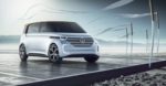
For around the end of the decade, Dr Diess presented the BUDD-e. This is a long-distance electric car (233-mile range) in a CUV format which can be charged to 80% capacity in 30 minutes. The batteries lay flat in the floor providing increased cabin/baggage space and increased stability (Mary Barra of GM described similar battery distribution for the Chevy Bolt EV). Distinctive features include no more door handles (doors open with the wave of a hand) and a completely electronic cockpit where display info can be moved back and forth (using hand gestures again) between driver and the infotainment screens.
They have also partnered with LG and DoorBird who are big in home automation capabilities to connect home automation features to the car. So you can answer a video doorbell for example or open your door for guests. I’m not so sure this is an advance – more driver distractions and I would rarely want to open my door remotely to anyone, but they still have time to iron out the kinks, I hope. One last cool feature – mail (physical mail and packages) can be delivered to the car. There’s a tray in the back a postal or other service can open to drop in packages. Not sure how they’ll get agreement on that one with delivery services, but an interesting direction.
The long-range view is based on autonomy: self-driving, self-parking, self charging cars which inter-communicate to avoid accidents and congestion. No time-line put on this one. Dr Diess did share a couple of interesting pieces of information. VW has acquired, with BMW and Daimler (the big 3 in Germany), the Nokia digital maps and location services. This will be an important part of their direction in autonomy. And at this CES, they signed an MOU with Mobileye focusing on environmental-mapping (around the car) technology. (This doesn’t help the view that Mobileye have peaked – they seem to be going from strength to strength.)
Finally, Dr Diess wrapped-up by repeating his apology and the VW commitment to get agreement in the US on acceptable solutions to diesel emission problems followed by quick implementation of those solutions for US customers. I have to say his presentation was a solid performance under challenging circumstances. I look forward to hearing more from the VW group in the future.